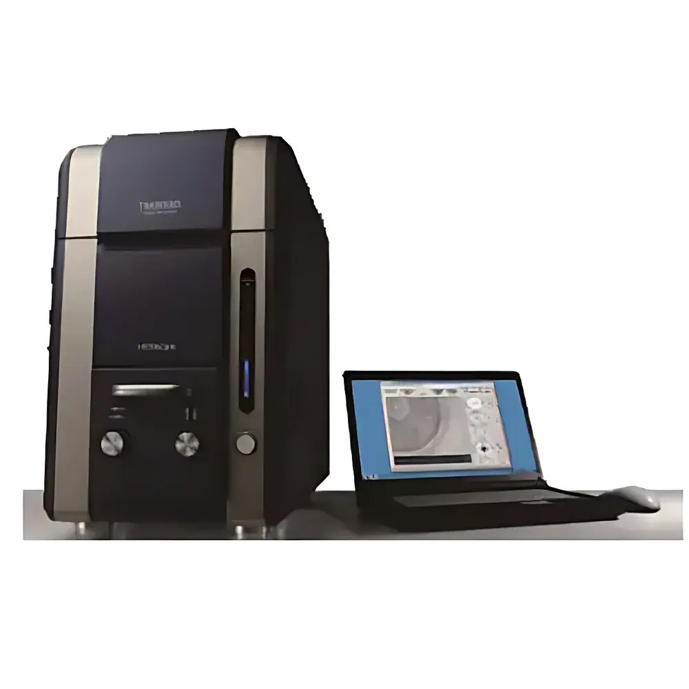

BM TM3030 Desktop Scanning Electron Microscope
| Brand | BM |
|---|---|
| Origin | Shanghai, China |
| Model | TM3030 |
| Instrument Type | Desktop SEM |
| Electron Source | Pre-aligned Tungsten Filament |
| Accelerating Voltages | 5 kV, 15 kV |
| Magnification Range | 15× to 30,000× (with digital zoom: 2×, 4×) |
| Maximum Sample Diameter | 70 mm |
| Sample Stage Travel | X: ±17.5 mm, Y: ±17.5 mm |
| Detector System | High-sensitivity 4-segment semiconductor backscattered electron (BSE) detector |
| Vacuum System | Turbo-molecular pump (30 L/s), diaphragm pump (1 m³/h), ultimate vacuum ≤1.5×10⁻⁵ Pa, variable pressure mode (6–270 Pa, 22 steps) |
| Control Interface | Two USB 2.0 ports, Ethernet port |
| Operating System | Microsoft Windows® 7 or later |
| Display | 15.4-inch LCD (1280×800 resolution) |
| Auto-functions | Auto filament saturation, auto beam alignment, auto stigmation, auto focus, auto brightness/contrast, overcurrent protection, leakage circuit breaker |
Overview
The BM TM3030 Desktop Scanning Electron Microscope (SEM) is an entry-level, compact, and fully integrated analytical instrument engineered for routine surface imaging and compositional analysis in academic laboratories, quality control environments, and industrial R&D settings. It operates on the principle of scanning a focused electron beam across a conductive or coated sample surface and detecting secondary electrons (SE) and backscattered electrons (BSE) to generate high-resolution topographic and atomic-number-contrast images. Unlike conventional floor-standing SEMs requiring dedicated shielded rooms and extensive infrastructure, the TM3030 features a self-contained vacuum system with automated pneumatic valve control, enabling rapid pump-down and stable operation within standard laboratory environments (15–30°C, 40–70% RH). Its pre-aligned tungsten thermionic electron source delivers consistent beam current and long filament life—ideal for users prioritizing operational simplicity without compromising fundamental imaging fidelity.
Key Features
- Compact desktop architecture: Fully integrated main unit (63–66 kg), turbo-molecular and diaphragm pumping system, and control PC in a single footprint (330 × 606 × 565 mm), eliminating need for external chillers or high-power electrical upgrades.
- Automated electron optics workflow: Includes factory-calibrated auto filament saturation, auto beam alignment, auto stigmation, auto focus, and auto brightness/contrast—reducing operator dependency and minimizing training time for new users.
- Dual-mode imaging capability: Supports standard mode (optimized for SE contrast), charge-reduction mode (for non-conductive or beam-sensitive specimens), and high-current analysis mode (enhanced signal-to-noise for EDS integration).
- Multi-contrast imaging: Generates morphological (SE), compositional (BSE), and topographic (in-lens BSE variants) images—including dual BSE channel mapping (BSE1/BSE2) and relief-enhanced “relief” mode—without hardware reconfiguration.
- Robust vacuum management: Variable-pressure operation (6–270 Pa, 22 discrete steps) enables direct observation of hydrated, insulating, or outgassing samples without metal coating; ultimate high-vacuum performance ≤1.5×10⁻⁵ Pa supports high-resolution imaging of conductive specimens.
- Integrated safety architecture: Built-in overcurrent protection and earth-leakage circuit breaker comply with IEC 61010-1 safety standards for laboratory electrical equipment.
Sample Compatibility & Compliance
The TM3030 accommodates specimens up to 70 mm in diameter and 50 mm in height, with manual XY stage travel of ±17.5 mm per axis. Its variable-pressure vacuum mode allows direct imaging of biological tissues, polymers, ceramics, and uncoated powders—reducing or eliminating the need for sputter coating. The high-sensitivity 4-segment semiconductor BSE detector enables quantitative atomic number (Z)-contrast mapping, supporting semi-quantitative elemental distribution assessment when paired with optional energy-dispersive X-ray spectroscopy (EDS) modules. While the base system does not include full EDS hardware, its standardized EDX interface (at WD = 10 mm, TOA = 35°) ensures compatibility with third-party detectors conforming to ISO 22309 and ASTM E1508 guidelines for microanalysis. All vacuum, power, and thermal specifications meet CE marking requirements under Directive 2014/30/EU (EMC) and 2014/35/EU (LVD). Data acquisition and storage protocols support GLP-compliant audit trails when used with validated software configurations.
Software & Data Management
Control and image acquisition are managed via a dedicated Windows® 7 (or later) workstation with Intel® Core™2 Duo or equivalent CPU and ≥2 GB RAM. The native software suite provides real-time TV-scan (640×480, 25 fps), fast-scan (6.3 fps), and slow-scan modes (0.5–40 sec/frame) for optimizing signal-to-noise ratio across diverse sample types. Image data are saved in industry-standard formats (BMP, TIFF, JPEG) at resolutions of 640×480 or 1280×960 pixels, with embedded metadata including magnification, working distance, acceleration voltage, date/time stamp, scan speed, detector mode, and user annotations. On-screen measurement tools support line, angle, and area quantification with calibrated micrometer scale overlays. Optional software modules enable batch image export, basic 3D surface reconstruction from tilt-series, and DICOM-compatible export for cross-platform archival. All system logs—including vacuum status, beam parameters, and user actions—are timestamped and stored locally, facilitating internal validation and FDA 21 CFR Part 11 compliance when deployed with electronic signature and access-control add-ons.
Applications
- Materials science: Fracture surface analysis of metals and alloys, particle size/distribution assessment in catalysts and battery electrode materials, coating uniformity verification.
- Life sciences: Imaging of freeze-dried or critical-point-dried biological specimens (e.g., pollen, diatoms, insect cuticles), vascular network visualization in plant tissues.
- Geology & forensics: Mineral phase identification via BSE contrast, gunshot residue (GSR) morphology and elemental correlation, fiber and paint chip characterization.
- Electronics & semiconductors: PCB trace inspection, solder joint integrity evaluation, contamination identification on wafer surfaces (with appropriate sample preparation).
- Quality assurance: Routine incoming inspection of raw materials, in-process monitoring of additive manufacturing builds, failure analysis of polymer components.
FAQ
Is the TM3030 compatible with energy-dispersive X-ray spectroscopy (EDS)?
Yes—the instrument includes a standardized EDX port positioned at 10 mm working distance and 35° take-off angle, enabling integration with commercial EDS detectors that adhere to common mechanical and electrical interface specifications.
What vacuum level is required for high-resolution imaging?
For optimal secondary electron resolution below 5 nm, operation at ≤1.5×10⁻⁵ Pa is recommended using the turbo-molecular pump. Variable-pressure mode (6–270 Pa) is reserved for charge-prone or volatile samples where resolution trade-offs are acceptable.
Can non-conductive samples be imaged without sputter coating?
Yes—charge-reduction mode and variable-pressure operation allow direct imaging of many insulators (e.g., plastics, ceramics, biological tissues), though resolution and signal stability may vary depending on specimen geometry and beam sensitivity.
Does the system support automated stage movement?
The standard configuration includes a manual XY stage. A motorized stage option is available as a factory-installed upgrade, providing programmable positioning and tiled-image stitching capability.
What regulatory standards does the TM3030 meet?
The system complies with CE directives for electromagnetic compatibility (2014/30/EU) and low-voltage safety (2014/35/EU); vacuum and thermal design follows ISO 14644-1 Class 8 cleanroom recommendations for lab-integrated instrumentation.


