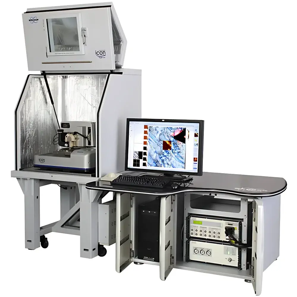
Bruker Dimension Icon Atomic Force Microscope
| Brand | Bruker |
|---|---|
| Origin | Germany |
| Manufacturer Type | Authorized Distributor |
| Origin Category | Imported |
| Model | Dimension Icon |
| Price Range | USD 135,000 – 205,000 (est.) |
| Instrument Type | Atomic Force Microscope |
| Application Class | Industrial-Grade AFM |
| XY Positional Noise | ≤ 0.15 nm (RMS) |
| Z-Noise Floor | 35 pm (RMS) |
| Sample Diameter Capacity | 210 mm (vacuum chuck) |
| Maximum Sample Thickness | ≤ 15 mm |
| Scan Area | 180 mm × 150 mm (motorized stage travel) |
Overview
The Bruker Dimension Icon Atomic Force Microscope is an industrial-grade scanning probe microscope engineered for high-resolution topographic, mechanical, and electrical characterization at the nanoscale. Based on contact, tapping, and advanced dynamic modes—including PeakForce Tapping®, ScanAsyst®, and Electrostatic Force Microscopy (EFM)—the system operates on a robust, low-drift platform optimized for reproducible quantitative nanomechanical mapping under ambient, liquid, or controlled environmental conditions. Its design integrates decades of Bruker’s AFM expertise with precision-machined optics, active vibration isolation, and thermally stable mechanical architecture to deliver sub-angstrom Z-noise performance (35 pm RMS) and ultra-low XY drift (≤0.15 nm RMS), enabling reliable long-term imaging and force spectroscopy on large-area substrates without compromise in resolution or fidelity.
Key Features
- Industrial-class motorized sample stage with 180 mm × 150 mm travel range, supporting automated multi-region acquisition and batch analysis across wafers, battery electrodes, photovoltaic films, and flexible electronics.
- Vacuum-chuck sample holder accommodating up to 210 mm diameter substrates with ≤15 mm thickness—compatible with semiconductor, display, and energy storage device inspection protocols.
- Closed-loop piezoelectric scanner architecture delivering true positional accuracy and linearity across full scan ranges, eliminating image distortion inherent in open-loop systems while maintaining low intrinsic noise (<35 pm Z-RMS).
- Modular signal routing and customizable detection electronics enabling real-time integration of external stimuli (e.g., bias voltage, temperature control, optical excitation) for correlative multimodal experiments.
- Intuitive, context-aware software interface with guided workflow modules—from initial tip approach and mode selection to parameter optimization and report generation—designed to reduce operator dependency and accelerate method development.
Sample Compatibility & Compliance
The Dimension Icon supports a broad spectrum of rigid and soft materials, including silicon wafers, graphene, perovskite thin films, polymer electrolytes, biological membranes, and conductive composites. Its vacuum-compatible stage and optional environmental enclosure meet requirements for cleanroom-integrated metrology workflows. The system complies with ISO/IEC 17025 calibration traceability frameworks when used with certified reference standards (e.g., NIST SRM 2461, 2462). Data integrity features—including user-access logging, audit trail recording, and electronic signature support—are configurable to align with GLP, GMP, and FDA 21 CFR Part 11 regulatory expectations for quality-controlled R&D and process validation environments.
Software & Data Management
NanoScope Analysis v3.0+ provides comprehensive post-processing tools for quantitative surface metrology (ISO 25178 parameters), nanomechanical property extraction (modulus, adhesion, deformation), and statistical mapping visualization. Raw data is stored in vendor-neutral HDF5 format with embedded metadata (timestamp, instrument configuration, calibration history), facilitating interoperability with Python-based analysis pipelines (e.g., SciPy, scikit-image) and LIMS integration. Scripting APIs (Tcl/Tk, Python) enable automation of repetitive tasks such as grid-based defect review, cross-sectional profiling, or time-lapse nanomechanical monitoring—critical for reliability testing in battery cycling or OLED degradation studies.
Applications
- Nanomaterials R&D: Quantitative morphology and phase segregation analysis in organic photovoltaics, solid-state electrolytes, and 2D heterostructures.
- Semiconductor Process Control: Line-edge roughness (LER), trench profile metrology, and gate oxide uniformity assessment on 200–300 mm wafers.
- Energy Storage: In situ and operando mapping of SEI evolution, lithium dendrite nucleation, and electrode particle cracking during electrochemical cycling.
- Life Sciences: High-resolution structural imaging of membrane proteins, extracellular vesicles, and hydrogel scaffolds under physiological buffer conditions.
- Advanced Manufacturing: Surface finish verification of micro-optical components, MEMS devices, and additive-manufactured metal parts per ASTM E2923 and ISO 21254 standards.
FAQ
Does the Dimension Icon support in situ electrochemical AFM (EC-AFM)?
Yes—the system accommodates commercial electrochemical cells and potentiostat integration via analog I/O and synchronized trigger routing, enabling concurrent topography and current mapping during battery or corrosion studies.
Is the vacuum chuck compatible with non-conductive or fragile substrates?
Yes—adjustable vacuum pressure and optional soft-seal gaskets prevent damage to brittle or low-modulus samples such as perovskite solar cells or polymer films.
Can third-party probes be used without compromising closed-loop performance?
All commercially available AFM probes with standard holders (e.g., Olympus AC240TS, BudgetSensors Tap150Al-GS) are supported; calibration routines automatically compensate for cantilever-specific spring constants and optical lever sensitivity.
What level of technical support and service coverage is available globally?
Bruker offers factory-certified field service engineers, remote diagnostics, annual preventive maintenance contracts, and application-specific training programs aligned with ISO 9001 service management standards.
How does the Dimension Icon differ from the Dimension FastScan or Edge models?
The Icon prioritizes large-area industrial throughput and environmental stability over ultra-high-speed imaging (FastScan) or entry-level cost optimization (Edge), making it the preferred platform for metrology-critical production R&D labs requiring traceable, repeatable nanoscale characterization.


