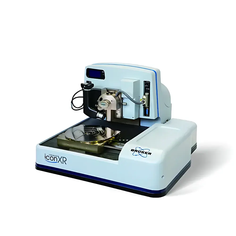
Bruker Dimension XR Scanning Probe Microscope
| Brand | Bruker |
|---|---|
| Origin | Germany |
| Model | Dimension XR |
| Instrument Type | Scanning Tunneling Microscope (STM) / Atomic Force Microscope (AFM) Platform |
| Maximum Sample Diameter | 210 mm (vacuum chuck), Thickness ≤ 15 mm |
| Environmental Operation Modes | Ambient air, liquid, electrochemical cell |
Overview
The Bruker Dimension XR is a high-performance, multi-environment scanning probe microscope (SPM) platform engineered for quantitative nanoscale characterization across mechanical, electrical, electrochemical, and topographic domains. Built upon Bruker’s decades-long leadership in SPM innovation, the Dimension XR integrates proprietary PeakForce Tapping® technology with an ultra-stable mechanical architecture, enabling atomic-resolution imaging and nanomechanical mapping under ambient, liquid, and controlled electrochemical conditions. Unlike conventional AFMs limited to qualitative or low-bandwidth quantitative modes, the Dimension XR delivers true quantitative nanodynamics—supporting linear viscoelastic measurements across a frequency range of 0.1 Hz to 20 kHz via its nDMA-AFM (nano-Dynamic Mechanical Analysis) module. This capability bridges the gap between macroscopic DMA and nanoscale material response, yielding storage modulus (E′), loss modulus (E″), and tan δ values directly comparable to bulk rheological standards (e.g., ASTM D7028, ISO 6721-4). Its dual-channel detection, phase-drift compensation, and reference-frequency tracking ensure measurement fidelity at sub-nanometer force setpoints—even on soft, heterogeneous, or hydrated samples.
Key Features
- PeakForce Tapping® with real-time force control: Enables simultaneous topography, adhesion, deformation, dissipation, and modulus mapping at sub-nanometer resolution on polymers, biomaterials, oxides, and composites.
- nDMA-AFM module: Quantifies nanoscale viscoelasticity in the linear strain regime; supports frequency sweeps from 0.1 Hz to 20 kHz; outputs E′, E″, and tan δ aligned with macroscopic DMA conventions.
- DataCube mode: Acquires full force-distance spectra at every pixel using rapid force array (RFA) acquisition; user-defined dwell time enables concurrent electrical (I-V, C-V) and mechanical spectroscopy per pixel—uniquely available on commercial SPM platforms.
- Electrochemical SPM (EC-SPM): Combines PeakForce Tapping with potentiostatic control for in situ/operando nanoscale electrochemical imaging; achieves lateral resolution <10 nm in aqueous electrolytes—orders of magnitude beyond conventional SECM or SKP.
- Ultra-stable metrology-grade frame: Active vibration isolation, low-drift piezo scanners, and thermal drift compensation enable repeatable atomic-resolution imaging over >100 consecutive scans—even on rough substrates such as float glass or oxidized silicon.
- Modular environmental compatibility: Fully integrated sample stages support vacuum-chuck mounting (up to 210 mm Ø, ≤15 mm thick), fluid cells, electrochemical cells, and temperature-controlled enclosures.
Sample Compatibility & Compliance
The Dimension XR accommodates a broad spectrum of sample types—including conductive and insulating thin films, battery electrode cross-sections, polymer blends, biological membranes, corrosion interfaces, and 2D materials—without requiring conductive coating. Its vacuum-chuck stage ensures flatness and positional repeatability for large-area metrology applications (e.g., wafer-scale defect analysis per SEMI F20). For regulated environments, the system supports audit-ready operation under GLP/GMP frameworks: raw data files include embedded metadata (timestamp, operator ID, instrument configuration, calibration history), and optional software modules comply with FDA 21 CFR Part 11 requirements for electronic records and signatures. All nDMA-AFM and EC-SPM protocols are traceable to ISO/IEC 17025-accredited calibration practices for force and displacement sensors.
Software & Data Management
NanoScope Analysis v3.6+ provides unified control for all imaging and spectroscopy modes, including automated tip qualification, batch processing of DataCube datasets, and export to HDF5 or MTEX-compatible formats for third-party modeling (e.g., finite-element simulation of local modulus distributions). The software embeds built-in statistical tools for spatial correlation analysis (e.g., autocorrelation of adhesion maps), machine-learning-assisted phase segmentation, and compliance with ASTM E2923 (Standard Guide for Nanotechnology Characterization) reporting templates. Raw data is stored in Bruker’s proprietary .spm format—with open-source Python libraries (e.g., pySPM) available for programmatic access and integration into laboratory information management systems (LIMS).
Applications
- Nanomechanics of energy materials: Quantifying local modulus gradients across solid-electrolyte interphases (SEI) in Li-ion batteries; mapping viscoelastic relaxation in polymer electrolytes during cycling.
- Corrosion science: In situ observation of pit initiation and passive film breakdown at nanometer scale under potentiodynamic control.
- Biointerface engineering: High-resolution mapping of ligand-receptor binding forces on functionalized surfaces; nanomechanical profiling of extracellular matrix stiffness gradients.
- Advanced polymers & composites: Correlating molecular-scale defects (e.g., chain entanglement density, crystallite boundaries) with bulk DMA performance through nDMA-AFM cross-validation.
- 2D materials & heterostructures: Simultaneous topographic, work-function, and interlayer shear modulus mapping on graphene/MoS₂ stacks in inert gas or liquid environments.
FAQ
Does the Dimension XR support true STM operation?
Yes—the system includes a dedicated STM head option with sub-angstrom Z-resolution and ultra-low noise current preamplifiers (<1 fA/√Hz), enabling atomic-resolution tunneling on conductive surfaces in UHV or ambient conditions.
Can nDMA-AFM data be correlated with bulk DMA results?
Yes—Bruker provides protocol documentation and calibration workflows that align nano-scale storage/loss moduli with ASTM D7028 and ISO 6721-4 standards, facilitating direct cross-scale validation.
Is electrochemical SPM compatible with standard three-electrode cells?
Yes—the EC-SPM module integrates seamlessly with commercially available electrochemical cells (e.g., BASi, Pine Research) and supports potentiostatic/galvanostatic control via analog I/O synchronization.
What sample preparation is required for DataCube acquisition?
No special preparation is needed beyond standard AFM requirements; however, optimal signal-to-noise ratio for concurrent electrical-mechanical spectroscopy benefits from clean, low-capacitance tip–sample interfaces and shielded cabling.
How is system stability verified post-installation?
Bruker performs on-site metrological verification using NIST-traceable step-height standards and thermal drift benchmarks; annual recalibration services include scanner linearity, force calibration, and environmental chamber performance validation.


