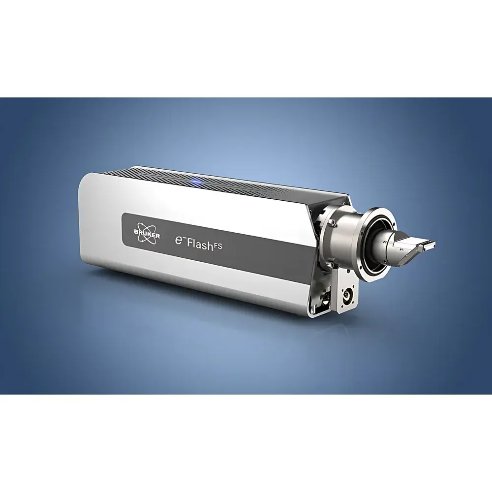
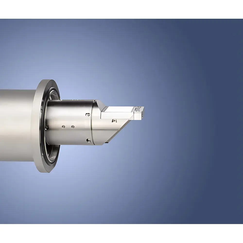
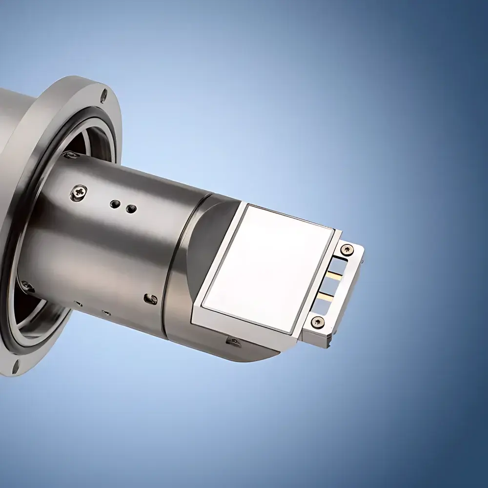
Bruker eflash FS EBSD System with Coaxial TKD OPTIMUS 2 and QUANTAX Detection Platform
| Brand | Bruker |
|---|---|
| Origin | Germany |
| Manufacturer Type | Authorized Distributor |
| Product Origin | Imported |
| Model | OPTIMUS 2 QUANTAX EBSD eflash FS |
| CCD Camera Resolution | 640 × 480 |
| Maximum Stage Speed | 10 mm/s |
| Spatial Resolution | 1.5 nm |
| Angular Resolution | 0.2° |
Overview
The Bruker eflash FS Electron Backscatter Diffraction (EBSD) system, integrated with the coaxial Transmission Kikuchi Diffraction (TKD) OPTIMUS 2 detector and QUANTAX energy-dispersive X-ray spectroscopy (EDS) platform, constitutes a high-precision, multi-modal microstructural characterization solution for scanning electron microscopes (SEM). Engineered for nanoscale crystallographic analysis, this system leverages both backscattered electron diffraction patterns (EBSPs) and transmitted Kikuchi patterns from thin foils or surface-near regions to deliver complementary orientation, phase, and strain information. The coaxial TKD geometry—unique among commercial TKD implementations—enables optimal signal collection in immersion lens SEM configurations, supporting ultra-high-resolution imaging modes without compromising pattern quality or acquisition speed. Unlike conventional off-axis TKD setups, the coaxial design minimizes geometric distortion and enhances pattern fidelity, particularly under low-kV (≤10 kV) and low-beam-current conditions (<1 nA), where nanoscale spatial resolution and high angular precision are critical.
Key Features
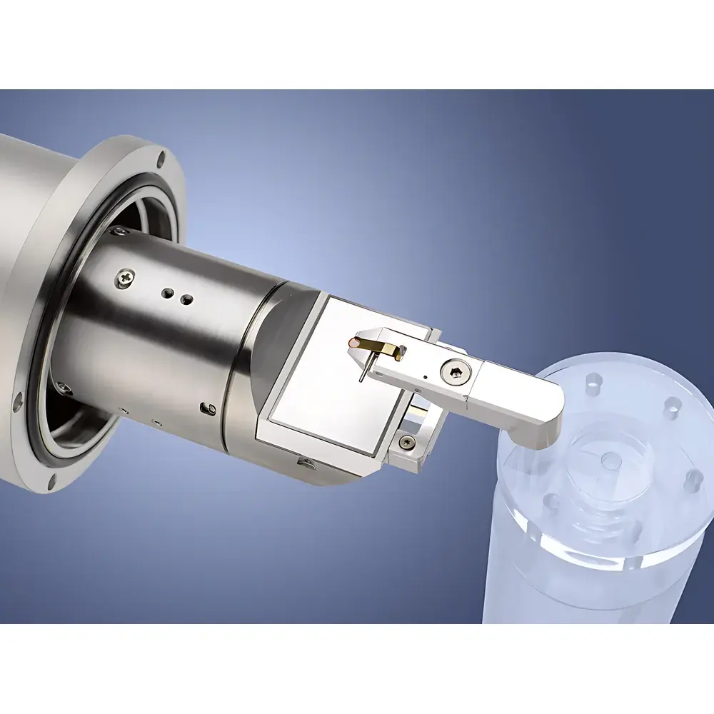
- Coaxial TKD OPTIMUS 2 detector: The only commercially available TKD solution fully compatible with immersion-mode SEMs, enabling seamless integration into high-resolution analytical workflows.
- eFlash FS high-speed EBSD camera: Delivers rapid pattern acquisition at frame rates optimized for dynamic microstructural mapping, with real-time indexing and confidence index evaluation.
- 1.5 nm spatial resolution: Achieved through optimized detector geometry, high-efficiency phosphor screen, and low-noise CMOS sensor architecture—validated under standard SEM operating conditions (e.g., 15–30 kV, 1–5 nA).
- 0.2° angular resolution: Supported by advanced pattern center calibration algorithms and sub-pixel Hough transform refinement, ensuring robust orientation differentiation in fine-grained or heavily deformed materials.
- Integrated ARGUS™ real-time imaging system: Provides automatic beam-sensitive sample monitoring, drift correction, and live pattern quality feedback during acquisition—essential for reproducible nanoscale EBSD/TKD mapping.
- QUANTAX EDS-EBSD correlation platform: Enables simultaneous chemical composition mapping and crystallographic phase identification with pixel-by-pixel data fusion, compliant with ASTM E1508 and ISO 14783 standards.
Sample Compatibility & Compliance
This system supports a broad range of conductive and non-conductive specimens—including metallic alloys, ceramics, geological thin sections, semiconductor wafers, and battery electrode cross-sections—when prepared via FIB-SEM lift-out or precision ion milling. For TKD operation, electron-transparent regions (typically <100 nm thick) are required; the coaxial geometry allows reliable pattern acquisition even from marginally transparent areas due to enhanced signal-to-noise ratio. All hardware and software modules comply with EU CE directives and meet electromagnetic compatibility (EMC) Class B requirements. Data handling protocols support GLP/GMP-aligned audit trails, and the system is configurable for FDA 21 CFR Part 11 compliance when deployed in regulated environments (e.g., medical device or pharmaceutical material qualification).
Software & Data Management
Acquisition and analysis are managed through Bruker’s ESPRIT software suite, which includes fully automated EBSD/TKD setup wizards, adaptive pattern indexing engines, and modular post-processing tools for grain reconstruction, misorientation analysis, and lattice strain quantification. Raw pattern datasets are stored in vendor-neutral HDF5 format, facilitating third-party interoperability (e.g., MTEX, Dream.3D). Metadata embedding adheres to the ICDD PDF-4+ and NIST SRM metadata schema, ensuring traceability across instrument platforms and laboratories. Batch processing pipelines support scheduled acquisitions, remote monitoring via secure HTTPS endpoints, and integration with laboratory information management systems (LIMS) via RESTful API.
Applications
- Nanoscale grain boundary engineering in additively manufactured alloys
- Crystallographic texture evolution during in-situ deformation experiments
- Phase transformation kinetics in lithium-ion cathode materials (e.g., NMC, LFP)
- Dislocation density mapping in semiconductor heterostructures using TKD-based geometric phase analysis (GPA)
- Strain partitioning at bi-material interfaces in thermoelectric composites
- Automated mineral phase identification and fabric analysis in petrographic thin sections
FAQ
What distinguishes coaxial TKD from conventional off-axis TKD configurations?
Coaxial TKD aligns the detector axis with the primary electron beam, eliminating parallax-induced pattern distortion and enabling stable pattern acquisition in immersion lens SEMs—where off-axis detectors suffer from reduced signal intensity and geometric instability.
Can the eflash FS system operate simultaneously with EDS and WDS?
Yes. The system is fully synchronized with Bruker QUANTAX EDS and optional WDS spectrometers via shared trigger logic and time-stamped metadata, allowing true correlative microanalysis.
Is TKD suitable for bulk samples, or does it require TEM-like specimen preparation?
TKD requires electron-transparent regions (typically ≤100 nm thickness), usually achieved via FIB-SEM sectioning or precision ion polishing—not bulk mounting. However, the coaxial design tolerates slightly thicker regions than off-axis alternatives.
How is angular resolution validated and maintained across different SEM platforms?
Angular resolution is verified using certified NIST-traceable Si and Ni reference standards, and maintained through routine pattern center calibration using the built-in ARGUS imaging feedback loop and motorized stage referencing.
Does the software support batch processing of large-area EBSD maps?
Yes. ESPRIT includes distributed computing support for multi-core CPU and GPU-accelerated indexing, with scalable storage options for terabyte-scale map datasets.


