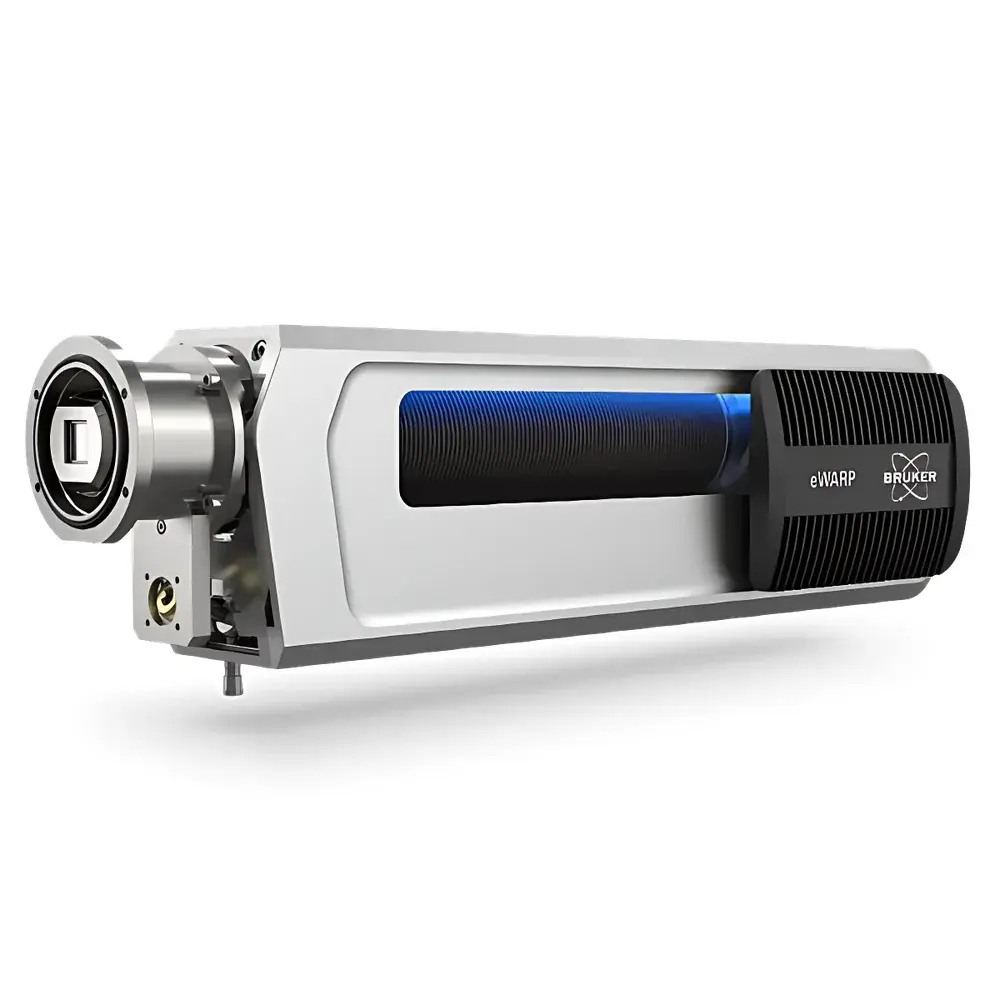
Bruker eWARP Electron Backscatter Diffraction (EBSD) System
| Brand | Bruker |
|---|---|
| Origin | Germany |
| Manufacturer Type | Authorized Distributor |
| Origin Category | Imported |
| Model | eWARP |
| Quotation | Upon Request |
| Maximum Pattern Acquisition Rate | 14,400 patterns/second |
| Spatial Resolution | 20 nm |
| Angular Resolution | 0.1° |
Overview
The Bruker eWARP Electron Backscatter Diffraction (EBSD) System is a high-performance, next-generation EBSD detector engineered for precision crystallographic orientation mapping in scanning electron microscopes (SEM). Operating on the fundamental principle of elastic backscattering of high-energy electrons from crystalline lattice planes—generating characteristic Kikuchi diffraction patterns—the eWARP system delivers quantitative microstructural data including grain orientation, phase identification, grain boundary character, and local strain estimation. Its design centers on maximizing pattern acquisition fidelity under low-voltage, low-beam-current conditions (e.g., 10 kV acceleration voltage and 12 nA beam current), enabling unprecedented spatial resolution without compromising pattern quality or indexing reliability. This capability directly addresses critical limitations in conventional EBSD, where higher accelerating voltages (e.g., 20 kV) increase interaction volume and degrade lateral resolution—particularly in beam-sensitive, nanoscale, or multiphase materials.
Key Features
- Ultra-high-speed acquisition: Sustained pattern capture at up to 14,400 patterns per second, enabling rapid large-area mapping, time-resolved in situ experiments, and efficient 3D EBSD tomography workflows.
- Sub-20 nm spatial resolution: Achieved via optimized low-voltage operation (10 kV standard), reducing electron interaction volume and enhancing Kikuchi band contrast—critical for resolving ultrafine microstructures such as martensite laths, battery cathode particles, and nanocrystalline alloys.
- High angular resolution of 0.1°: Ensures precise discrimination of small orientation gradients, enabling accurate misorientation analysis and reliable identification of low-angle boundaries and deformation substructure.
- Enhanced signal sensitivity: Advanced phosphor-scintillator architecture and low-noise CMOS sensor enable robust pattern detection under minimal beam dose—reducing sample damage and extending applicability to beam-sensitive materials including Li-ion battery cathodes (e.g., NCM, NCA), polymers, and thin-film heterostructures.
- Seamless integration with Bruker ESPRIT software: Full support for real-time indexing, confidence index calculation, phase identification, grain reconstruction, and advanced post-processing (e.g., GOS, IQ, grain boundary trace analysis) with >99% indexing success rate under optimized low-kV conditions.
Sample Compatibility & Compliance
The eWARP system is compatible with standard SEM platforms equipped with EBSD-compatible stage geometry and vacuum interfaces (including FEI/Thermo Fisher, Zeiss, JEOL, and Hitachi systems). It supports routine analysis of conductive and semi-conductive samples prepared via standard metallographic polishing, ion milling, or FIB-SEM lift-out. For non-conductive or beam-sensitive specimens—including battery electrode materials, geological minerals, and biological composites—low-kV operation minimizes charging and decomposition artifacts. The system complies with ISO/IEC 17025 requirements for analytical instrument validation and supports GLP/GMP-aligned workflows through ESPRIT’s audit-trail-enabled data logging, user access control, and electronic signature functionality per FDA 21 CFR Part 11 guidelines.
Software & Data Management
ESPRIT software serves as the unified platform for eWARP data acquisition, processing, and reporting. It provides automated calibration, dynamic background correction, and adaptive indexing algorithms trained on multi-phase reference databases (including ICDD PDF-4+ and Bruker’s proprietary crystallographic libraries). Raw pattern datasets are stored in standardized HDF5 format, ensuring long-term archival integrity and interoperability with third-party tools (e.g., MTEX, Dream.3D). Batch processing pipelines support statistical grain analysis (size, shape, aspect ratio, boundary type distribution), texture quantification (ODF, pole figures), and correlative analysis with EDS and CL data. All processing steps—including mask application, confidence thresholding, and grain merging—are fully traceable and reproducible.
Applications
- Battery materials R&D: Quantitative orientation mapping of NCM/NCA cathode particles (≈1–5 µm) at 20 nm step size reveals intra-particle misorientation, twin variants, and crack-initiating grain boundary networks—directly informing capacity retention and thermal runaway mechanisms.
- Advanced metallurgy: High-resolution characterization of martensitic stainless steels and Ti-6Al-4V, resolving individual laths and variant groups without image degradation from conventional 20 kV imaging.
- In situ mechanical testing: Real-time monitoring of dislocation nucleation, grain rotation, and twinning during nanoindentation or tensile straining inside SEM chambers.
- Geosciences and ceramics: Phase discrimination in multiphase rock thin sections and sintered oxide ceramics, leveraging high indexing reliability across abrupt compositional gradients.
- Additive manufacturing: Mapping epitaxial growth relationships, columnar-to-equiaxed transition zones, and residual stress fields in laser-powder bed fusion (LPBF) alloys.
FAQ
What accelerating voltage is recommended for optimal eWARP performance?
10 kV is the standard operational condition, delivering superior spatial resolution and indexing reliability while minimizing beam damage—especially for nanoscale and beam-sensitive materials.
Can eWARP be used with non-Bruker SEMs?
Yes—it integrates with major SEM platforms via standardized hardware interfaces and Bruker’s cross-platform ESPRIT software suite.
Is the 20 nm spatial resolution achievable across all material types?
Resolution is sample-dependent; it represents the system’s capability under optimal conditions (e.g., well-prepared martensitic steel or NCM cathodes at 10 kV), not a universal guarantee for all phases or surface qualities.
Does ESPRIT software support automated grain boundary classification?
Yes—boundaries are classified by misorientation angle and axis (e.g., Σ3 twin, random high-angle) using configurable thresholds aligned with ASTM E112 and ISO 26247 standards.
How does eWARP handle pattern distortion from sample tilt or topography?
ESPRIT incorporates real-time geometric correction algorithms based on calibrated detector-sample geometry and optional topographic input from simultaneous EDS or secondary electron imaging.


