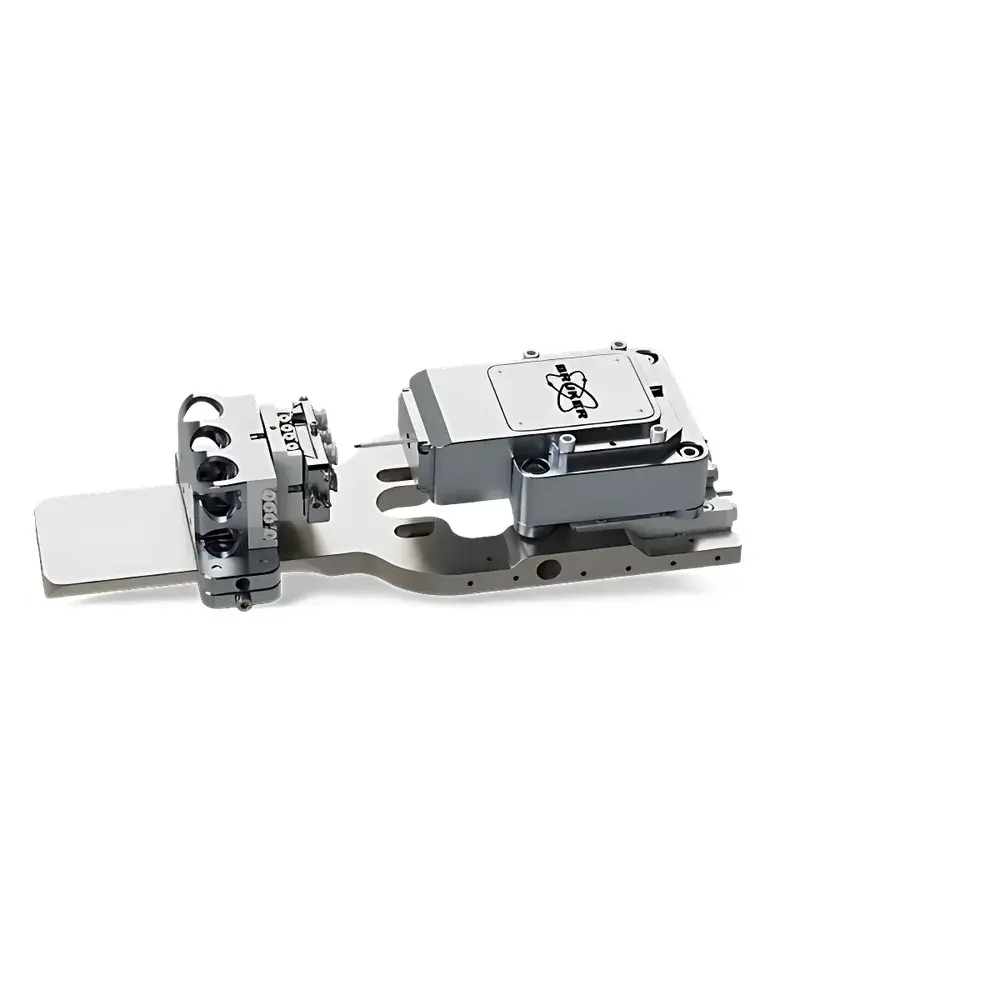
Bruker Hysitron PI 89 In-Situ SEM/FIB Nanomechanical Testing System
| Brand | Bruker |
|---|---|
| Origin | USA |
| Model | Hysitron PI 89 |
| Application | In-situ nanomechanical testing inside SEM and FIB/SEM chambers |
| Sensing Principle | Capacitive displacement sensing with sub-nanometer resolution |
| Actuation | Electromechanical force actuation |
| Force Range | Up to 100 mN (standard configuration) |
| Displacement Resolution | < 0.2 nm |
| Positioning Accuracy | ≤ 50 nm (with integrated linear encoder and motorized tilt/rotate stages) |
| Compatibility | Fully compatible with FEI/Thermo Fisher, Zeiss, JEOL, and Hitachi SEM/FIB platforms |
| Analytical Integration | Synchronized acquisition with EBSD, EDS, BSE, and TKD detectors |
Overview
The Bruker Hysitron PI 89 is a purpose-engineered in-situ nanomechanical testing system designed for direct integration within scanning electron microscope (SEM) and focused ion beam–SEM (FIB/SEM) chambers. It enables real-time, spatially correlated mechanical characterization—such as nanoindentation, microtensile testing, micropillar compression, microsphere compression, cantilever bending, fracture initiation, fatigue cycling, and dynamic mechanical analysis—while simultaneously acquiring high-resolution structural and compositional data. The system operates on a capacitive displacement sensing architecture, delivering sub-nanometer displacement resolution and high-force stability across its full 100 mN force range. Its modular design supports vacuum-compatible operation at pressures down to 1×10⁻⁶ mbar, ensuring compatibility with high-vacuum SEM environments without compromising imaging fidelity or mechanical measurement integrity.
Key Features
- Capacitive displacement transduction with <0.2 nm resolution and drift-compensated feedback control for quantitative mechanical property mapping.
- Integrated linear optical encoder for absolute position tracking, enabling repeatable sample navigation and precise correlation between mechanical test sites and SEM imaging coordinates.
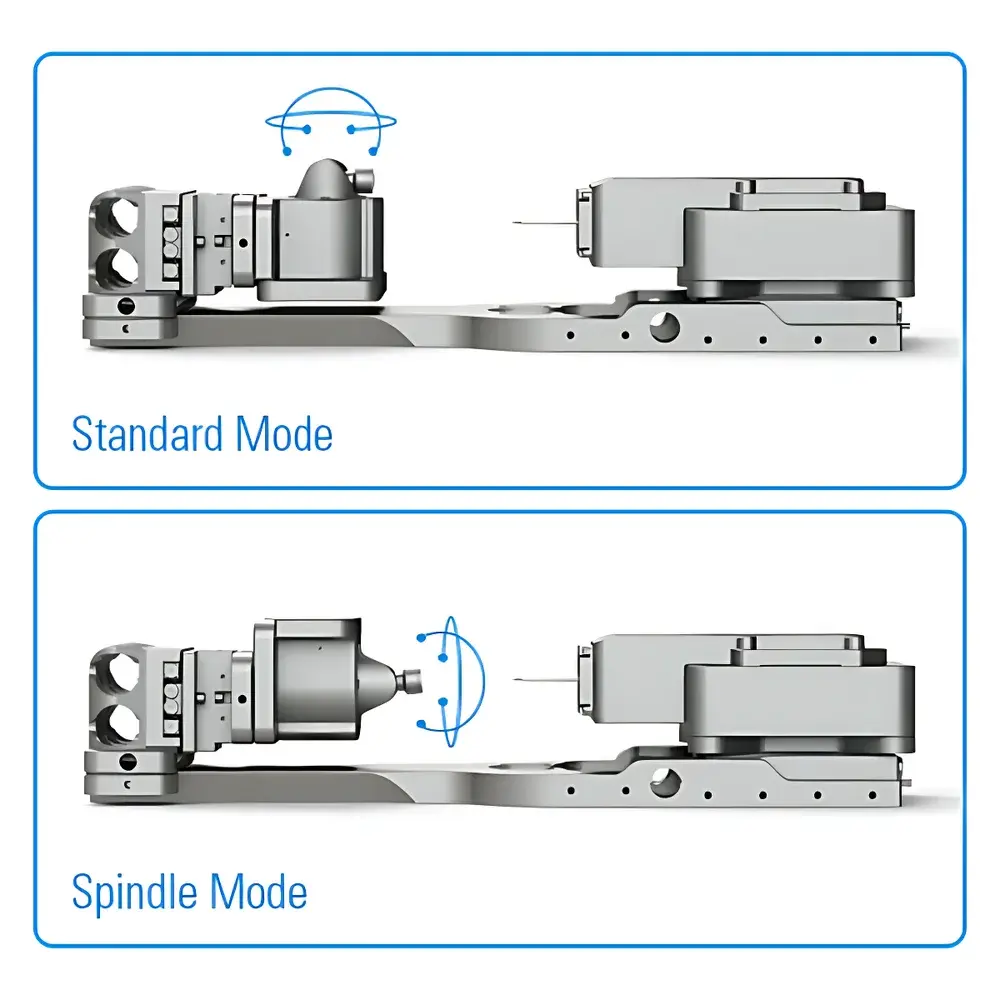
- Dual motorized rotation/tilt stage configurations (±90° tilt, 360° rotation) for multi-axis orientation control—critical for crystallographically aligned testing and post-test FIB sectioning.
- Real-time synchronization with SEM imaging systems and analytical detectors including backscattered electron (BSE), energy-dispersive X-ray spectroscopy (EDS), electron backscatter diffraction (EBSD), and transmission Kikuchi diffraction (TKD).
- Vacuum-rated, non-magnetic construction using titanium and ceramic components to minimize electromagnetic interference and thermal drift during extended in-chamber experiments.
- Modular probe cartridge system supporting interchangeable tips (Berkovich, cube-corner, flat-punch, spherical, tensile dogbones) for application-specific mechanical interrogation.
Sample Compatibility & Compliance
The PI 89 accommodates a broad range of conductive and semi-conductive specimens—including metallic alloys, ceramics, thin films, semiconductor heterostructures, and composite interfaces—without requiring conductive coating that may obscure surface features or alter mechanical response. Its compact footprint and low-profile mounting interface are engineered to fit standard SEM/FIB specimen holders and stage geometries. The system complies with ISO 14577-1:2015 (Metallic materials — Instrumented indentation test) for nanoindentation methodology, and supports traceable calibration protocols aligned with NIST-traceable reference standards. All mechanical data acquisition workflows adhere to GLP-compliant audit trail requirements when used with Bruker’s TriboScan software, including user authentication, parameter logging, and immutable result archiving per FDA 21 CFR Part 11 guidelines.
Software & Data Management
TriboScan software provides a unified platform for experiment design, real-time visualization, and post-processing of in-situ mechanical datasets. It supports synchronized acquisition triggers from SEM image frames or stage position signals, enabling pixel-by-pixel mechanical property mapping (e.g., hardness, modulus, creep, strain-rate sensitivity) overlaid directly onto SEM micrographs. Raw force–displacement curves, load-hold-unload segments, and time-series fatigue data are stored in HDF5 format with embedded metadata (stage coordinates, detector settings, vacuum status). Export options include ASTM E2546-compliant reporting templates, MATLAB-compatible .mat files, and CSV for third-party statistical analysis. Data provenance is preserved via timestamped operator logs, instrument configuration snapshots, and version-controlled analysis scripts.
Applications
- Quantitative nanoscale mechanical mapping of grain boundaries, phase interfaces, and intermetallic precipitates in aerospace alloys.
- In-situ observation of dislocation nucleation and pile-up during nanoindentation in single-crystal semiconductors.
- Mechanical reliability assessment of MEMS/NEMS device layers under controlled thermal or electrical bias.
- FIB-guided micropillar fabrication followed by uniaxial compression to determine size-dependent yield strength in nanocrystalline metals.
- Cyclic loading of battery electrode particles to correlate fracture evolution with electrochemical degradation pathways.
- Interfacial adhesion quantification in multilayer thin-film stacks using microscratch and blister testing modes.
FAQ
Is the PI 89 compatible with dual-beam FIB/SEM systems from Thermo Fisher and Zeiss?
Yes—the PI 89 is certified for integration with Thermo Fisher Helios Hybrids, Zeiss Crossbeam series, JEOL JIB-4000, and Hitachi MI4000 platforms via custom flange kits and chamber-specific alignment protocols.
Can the system perform quantitative tensile testing inside the SEM chamber?
Yes—microtensile specimens are fabricated in situ using FIB, then gripped and loaded using the PI 89’s dual-actuator tensile module; stress–strain curves are derived from calibrated force and DIC-based strain measurements.
Does the system support automated grid-based property mapping?
Yes—TriboScan includes scripting modules for autonomous positioning, indentation array execution, and EBSD-registered property overlay across predefined scan grids.
What calibration standards are recommended for routine verification?
Bruker supplies NIST-traceable fused silica and sapphire reference samples for displacement and force calibration; annual recalibration services are available through Bruker Metrology Centers.
How is electrical isolation maintained during concurrent EDS/EBSD acquisition?
All signal paths use shielded, differential cabling with galvanic isolation; the controller chassis is grounded separately from the SEM column ground to prevent noise coupling into spectral detectors.


