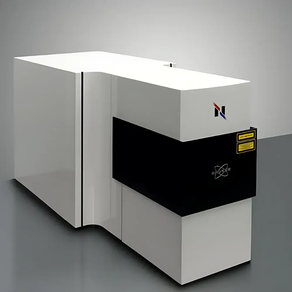
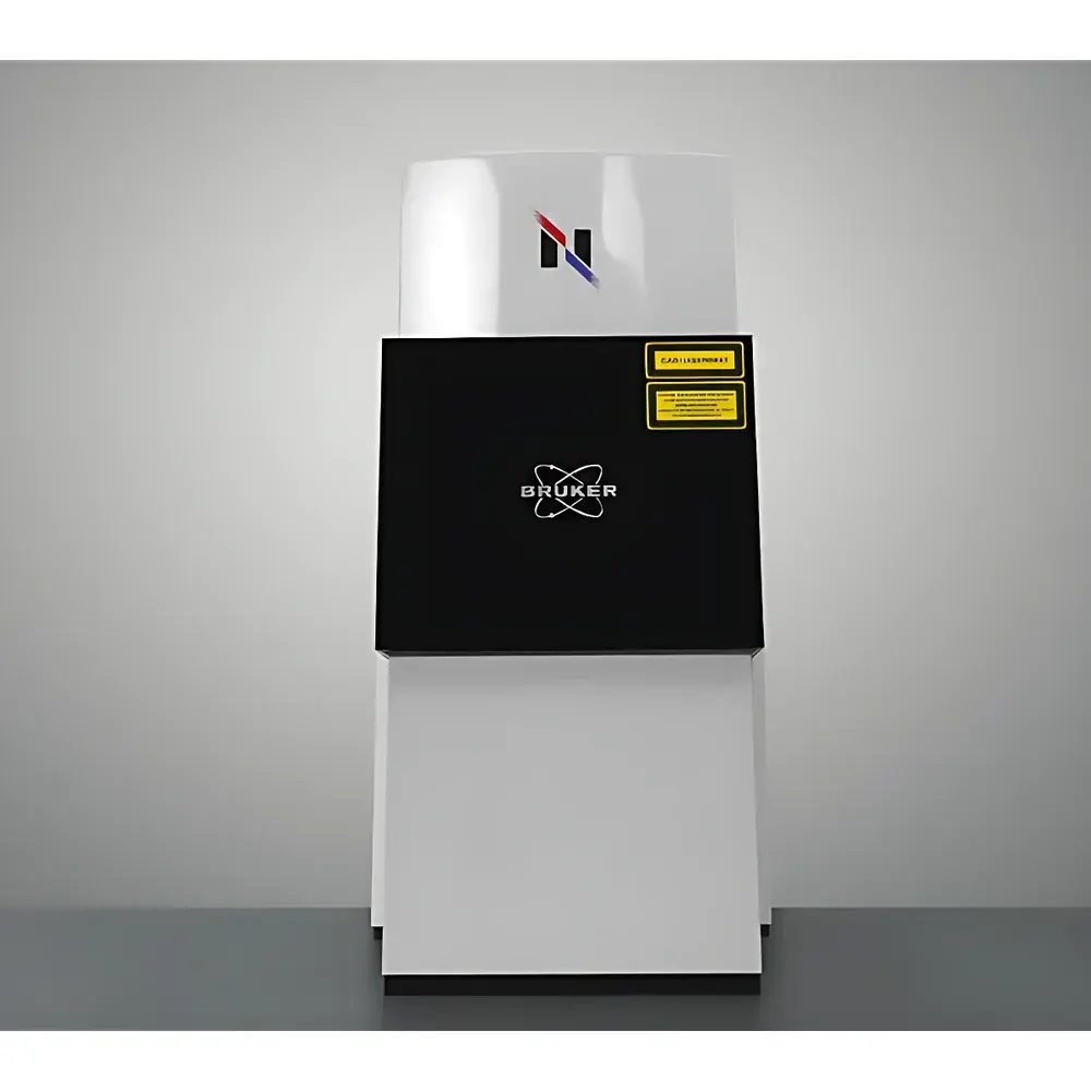
Bruker Nanophoton RAMANwalk Raman Microscope
| Brand | Bruker |
|---|---|
| Origin | Germany |
| Manufacturer Type | Authorized Distributor |
| Origin Category | Imported |
| Model | Nanophoton RAMANwalk |
| Instrument Type | Fourier Transform Raman Spectrometer |
| Spatial Resolution | 350 nm in X and Y |
Overview
The Bruker Nanophoton RAMANwalk is a high-performance confocal Raman microscope engineered for rapid, high-fidelity chemical imaging at submicron spatial resolution. Unlike conventional point-scanning or stage-scanning Raman systems, the RAMANwalk employs line-focused laser illumination coupled with a scientific-grade 2D CCD detector—enabling simultaneous acquisition of up to 400 spatially resolved Raman spectra per single exposure. This parallel detection architecture eliminates the trade-off between speed and spectral fidelity inherent in serial acquisition methods. The system operates on standard confocal Raman spectroscopy principles, utilizing monochromatic excitation (typically 532 nm or 785 nm lasers) and high-throughput transmission spectrographs with optimized grating dispersion and low-noise CCD readout. Its optical design conforms to ISO 17025-compliant alignment protocols and supports traceable calibration against NIST-traceable silicon and polystyrene standards.
Key Features
- Parallel spectral acquisition: Line-illumination geometry enables full-frame spectral capture without EMCCD amplification—reducing noise, eliminating gain-related artifacts, and preserving quantitative intensity linearity.
- Sub-diffraction spatial resolution: Achieves 350 nm lateral (X/Y) resolution and 1 µm axial (Z) resolution under optimal confocal conditions, validated per ISO 10110-5 and ASTM E2821 practices.
- High-speed hyperspectral mapping: Completes >100,000-pixel Raman images in minutes—not hours—using galvanometric mirror scanning with closed-loop position feedback and real-time spectral registration.
- Automated optical alignment: Integrated motorized optics enable self-alignment of excitation path, collection path, and spectrometer entrance slit—minimizing user intervention and ensuring reproducibility across operators and sessions.
- Modular laser platform: Supports multiple excitation wavelengths (532 nm, 633 nm, 785 nm) with automatic wavelength recognition, power stabilization, and safety interlocks compliant with IEC 60825-1 Class 3B requirements.
Sample Compatibility & Compliance
The RAMANwalk accommodates a broad range of solid, thin-film, and micro-particulate samples—including semiconductors, pharmaceutical polymorphs, battery cathode materials, geological inclusions, and biological tissue sections—without requiring conductive coating or vacuum. Its open-sample chamber design permits integration with environmental stages (temperature-controlled, humidity-regulated, or gas-purged). All firmware and hardware configurations adhere to EU CE marking directives, RoHS 2011/65/EU, and EMC Directive 2014/30/EU. Data acquisition workflows support audit trails and electronic signatures in accordance with FDA 21 CFR Part 11 and GLP/GMP documentation requirements when paired with Bruker’s OPUS software suite.
Software & Data Management
Controlled via Bruker’s OPUS 8.x platform with dedicated RAMANwalk module, the system provides fully automated acquisition scripting, multivariate spectral analysis (PCA, cluster analysis, MCR-ALS), and quantitative component mapping. Raw spectral data are stored in HDF5 format with embedded metadata (laser power, integration time, objective magnification, grating configuration), ensuring FAIR (Findable, Accessible, Interoperable, Reusable) compliance. Batch processing pipelines support spectral preprocessing (cosmic ray removal, baseline correction using asymmetric least squares), peak fitting (Voigt profiles), and correlation with complementary techniques (e.g., SEM-EDS, FTIR). Export options include ASCII, CSV, and vendor-neutral JCAMP-DX formats for third-party chemometric tools.
Applications
- Pharmaceutical solid-state characterization: Polymorph distribution mapping in tablet cross-sections and crystallinity profiling in amorphous dispersions.
- Materials science: Strain mapping in 2D transition metal dichalcogenides (TMDs), defect identification in graphene layers, and phase segregation analysis in perovskite solar cell films.
- Forensic trace evidence: Non-destructive identification of pigments, dyes, and illicit drug adulterants in micrometer-scale residues.
- Geosciences: In situ mineral assemblage quantification in polished thin sections under ambient conditions.
- Microelectronics: Contamination localization on wafer surfaces and interfacial reaction layer analysis in stacked dielectric structures.
FAQ
Is the RAMANwalk compatible with existing Bruker OPUS software licenses?
Yes—the system integrates natively with OPUS 8.2 or later and leverages existing instrument control modules and chemometric libraries without requiring additional license tiers.
Does it support depth profiling or 3D reconstruction?
Yes—z-stack acquisition is fully automated with piezo-driven objective focus; reconstructed 3D chemical volumes are generated using deconvolution algorithms compliant with ISO/IEC 17025 uncertainty propagation guidelines.
Can the system be upgraded to include time-resolved capabilities?
No—the RAMANwalk is optimized for steady-state Raman imaging; time-resolved measurements require pulsed excitation sources and TCSPC detection, which are outside its architectural scope.
What maintenance intervals are recommended for optical alignment verification?
Bruker recommends quarterly verification using the built-in auto-calibration routine and annual factory recalibration with NIST-traceable reference standards.
Related Products
")


")