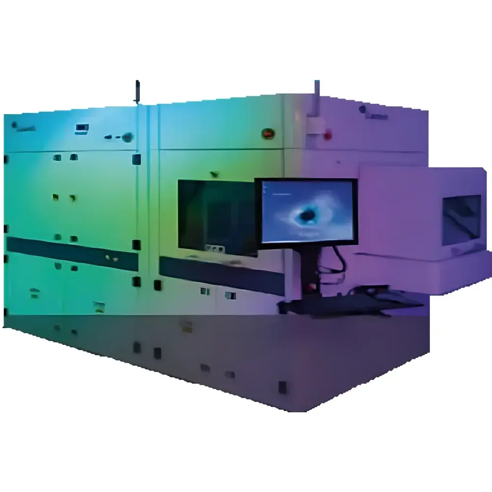
CAMTEK Eagle-I Advanced 2D Automatic Optical Inspection System for Semiconductor Wafer-Level Packaging
| Key | Origin: Imported |
|---|---|
| Manufacturer Type | Authorized Distributor |
| Model | Eagle-I |
| Inspection Speed | 50 million bump measurement points per wafer |
| 2D Detection Accuracy | 0.2 µm |
| 3D Height Measurement Accuracy | 0.05 µm (Measurement Range: 2–100 µm) |
Overview
The CAMTEK Eagle-I is a high-throughput, production-grade 2D Automatic Optical Inspection (AOI) system engineered specifically for semiconductor wafer-level packaging applications. It employs high-resolution industrial imaging coupled with proprietary real-time image acquisition and pixel-level analysis algorithms to detect surface anomalies, dimensional deviations, and pattern fidelity across advanced interconnect structures—including solder bumps (bumps), redistribution layers (RDL), under-bump metallization (UBM), vias, and critical dimension (CD) features on compound semiconductor and CMOS wafers. Unlike general-purpose AOI platforms, the Eagle-I integrates hardware-optimized optics, precision motion control, and application-specific defect classification logic calibrated for front-end-of-line (FEOL) post-plating, post-lithography, and post-dicing inspection workflows. Its architecture supports both rule-based and CAD-driven comparison methodologies, enabling traceable, repeatable pass/fail decisions aligned with semiconductor manufacturing process control requirements.
Key Features
- High-speed 2D inspection platform optimized for mass production environments—capable of acquiring and analyzing up to 50 million bump measurement points per single wafer pass.
- Sub-micron spatial resolution: 2D lateral detection accuracy of ±0.2 µm; 3D height metrology accuracy of ±0.05 µm within a 2–100 µm vertical range.
- Dual-mode inspection engine supporting both intensity-based anomaly detection and CAD-overlay pattern matching for RDL line width/spacing, bump coplanarity, and via fill verification.
- Multi-magnification optical path with motorized zoom lenses and adaptive focus control—enabling simultaneous macro-level defect screening and micro-feature metrology on warped or non-planar wafers.
- Robust mechanical design compliant with SEMI S2/S8 safety standards and cleanroom-compatible (Class 100 / ISO Class 5) enclosure construction.
- Real-time image sharpening and noise suppression firmware—enhancing contrast sensitivity for sub-0.2 µm surface scratches, residues, and bridging defects.
Sample Compatibility & Compliance
The Eagle-I accommodates standard silicon, glass, and compound semiconductor wafers ranging from 150 mm to 300 mm in diameter, including warped, thinned, or temporary-bonded substrates typical in fan-out wafer-level packaging (FOWLP) and 2.5D/3D IC integration processes. It supports inspection of copper pillar bumps, micro-bumps (<2 µm pitch), TSV openings, and fine-pitch RDLs fabricated using advanced lithography nodes (≤2 µm L/S). All inspection recipes are fully traceable and support audit-ready reporting per ISO 9001, IATF 16949, and SEMI E142 data integrity guidelines. System validation protocols include MSA (Measurement Systems Analysis) per AIAG MSA-4 and Gage R&R studies for critical parameters such as bump diameter, edge definition, and positional deviation.
Software & Data Management
Powered by CAMTEK’s proprietary Inspector™ software suite, the Eagle-I delivers integrated recipe management, defect classification hierarchy, and statistical process monitoring (SPC) dashboards. The software supports FDA 21 CFR Part 11-compliant user access controls, electronic signatures, and full audit trail logging—including parameter changes, operator actions, and calibration events. Raw image archives, defect maps, and metrology reports are stored in vendor-neutral formats (TIFF, CSV, XML) compatible with factory MES and yield management systems (e.g., PDF, Yield Explorer, Discover). Optional modules include automated defect review linkage with SEM/FIB tools via SECS/GEM interface and AI-assisted false-call reduction using supervised learning models trained on historical fab data.
Applications
- Post-electroplating bump inspection for height uniformity, shape fidelity, and bridging detection.
- RDL post-etch CD verification—line width, spacing, corner rounding, and edge roughness quantification.
- Probe mark size and morphology assessment during electrical test qualification (OQC).
- Post-dicing die surface inspection for chipping, cracking, and contamination on CMOS image sensors and MEMS devices.
- LED epitaxial wafer surface defect mapping—including pits, particles, and dislocation clusters affecting light extraction efficiency.
- TSV landing pad alignment and fill quality evaluation prior to micro-bump formation.
FAQ
What distinguishes the Eagle-I from CAMTEK’s Eagle-A and EagleT-i platforms?
The Eagle-I is purpose-built for high-volume 2D-only inspection with emphasis on throughput and repeatability in bump and RDL metrology; Eagle-A adds integrated 3D profilometry for height and coplanarity, while EagleT-i prioritizes ultra-high-speed scanning and multi-scale imaging for advanced node defect detection.
Does the Eagle-I support automatic defect classification (ADC)?
Yes—Inspector™ software includes configurable ADC rules based on size, shape, contrast, and spatial context, with optional supervised training for custom defect families.
Can the system integrate with existing fab automation infrastructure?
It supports standard SECS/GEM, HSMS, and OPC UA protocols for communication with host MES, AMHS, and equipment monitoring systems.
Is the Eagle-I qualified for use in GMP or ISO 13485-certified medical device manufacturing?
While primarily deployed in semiconductor fabs, its documentation package—including IQ/OQ/PQ protocols, calibration certificates, and change control records—meets baseline requirements for regulated environments when configured per customer validation scope.
What maintenance intervals and service coverage options are available?
Standard preventive maintenance is scheduled every 6 months; extended warranty and 24/7 remote diagnostics support are offered through CAMTEK’s global service network, with local field engineers available in North America, Europe, and Asia Pacific regions.


