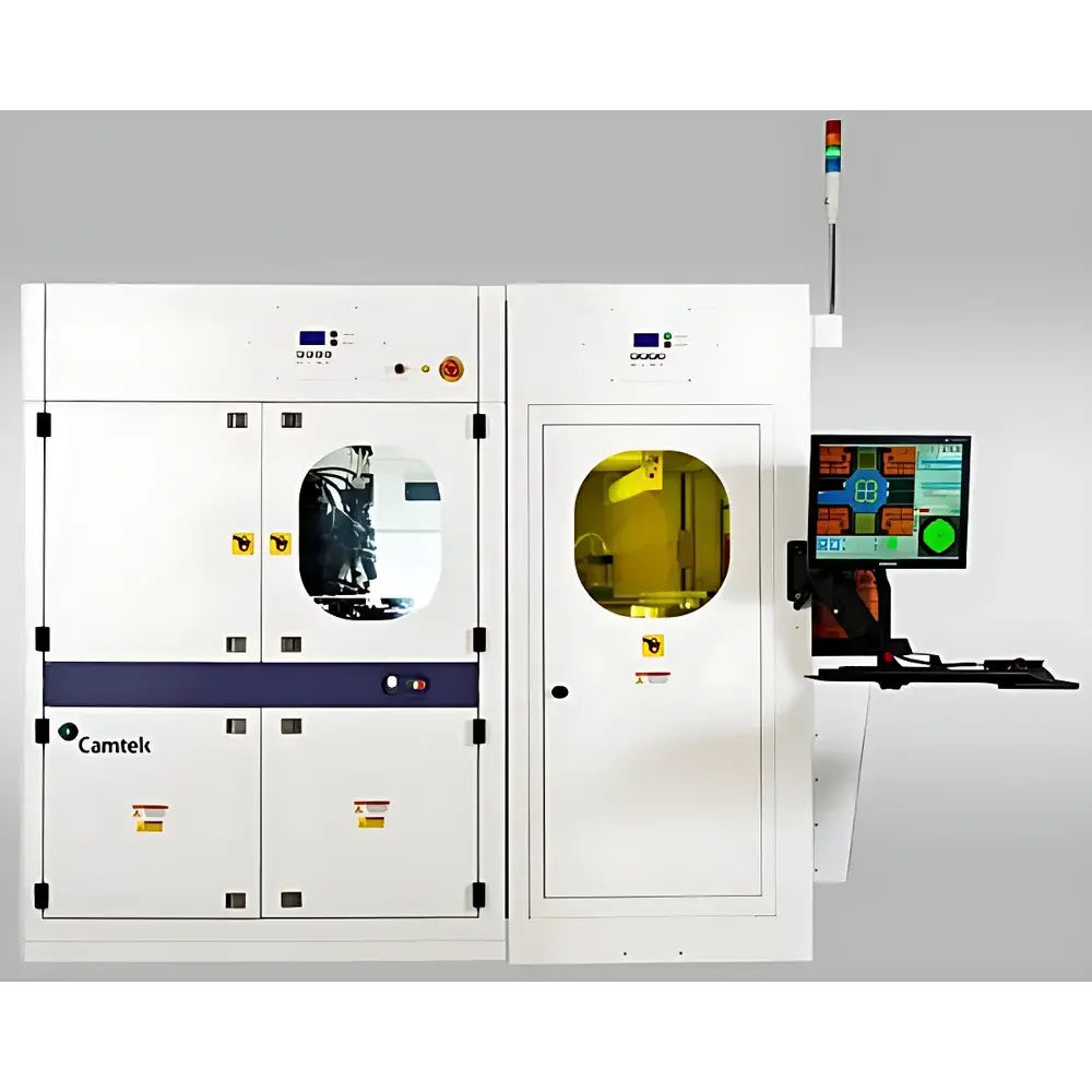
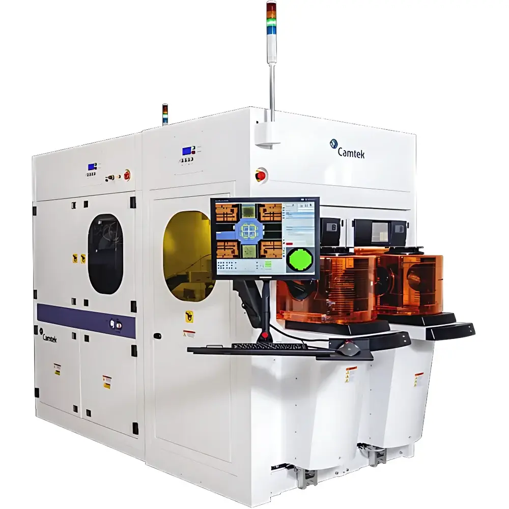
CAMTEK Eagle-I Series Advanced 2D/3D Automatic Optical Inspection System for Semiconductor Wafer-Level Packaging
| Origin | Imported |
|---|---|
| Manufacturer Type | Authorized Distributor |
| Model | CAMTEK Eagle-I / Eagle-AP / EagleT-i |
| Price Range | USD 650,000 – 1,050,000 |
| Inspection Throughput | Up to 50 million bump measurement points per wafer |
| 2D Detection Resolution | 0.2 µm |
| 3D Height Measurement Accuracy | ±0.05 µm (Measurement Range: 2–100 µm) |
| Minimum Detectable Feature Size | 2 µm bump / 2 µm line width |
| Defect Sensitivity | Down to 0.2 µm surface anomalies |
Overview
The CAMTEK Eagle-I Series represents a high-precision, production-grade Automatic Optical Inspection (AOI) platform engineered specifically for semiconductor wafer-level packaging and advanced interconnect metrology. Utilizing high-resolution industrial imaging coupled with proprietary real-time image processing architecture, the system performs non-contact, high-speed 2D pattern fidelity verification and 3D topographic profiling of critical structures including solder bumps (mBump, Cu pillar), redistribution layers (RDL), under-bump metallization (UBM), vias, and TSV fill profiles. Its optical detection principle is based on multi-angle bright-field/dark-field illumination, telecentric lensing, and pixel-registered CMOS sensor arrays — enabling sub-micron spatial resolution and robust defect classification across varying reflectivity, topology, and wafer warpage conditions (up to 2 mm bow). Designed for integration into front-end-of-line (FEOL) post-CMP/post-litho inspection and back-end-of-line (BEOL) post-plating/post-dicing workflows, the Eagle-I Series supports both rule-based and CAD-guided inspection methodologies compliant with industry-standard mask data formats (OASIS, GDSII).
Key Features
- Modular optical head configuration supporting simultaneous 2D intensity analysis and 3D height mapping via focus variation or structured light projection (Eagle-AP variant)
- Real-time sub-pixel registration engine with automatic wafer alignment compensation for thermal drift and mechanical stage instability
- Dual-mode illumination system: adjustable LED spectral bands (450–850 nm) optimized for metal vs. dielectric contrast enhancement
- High-throughput scanning architecture capable of acquiring and analyzing >50 million discrete bump measurement points per 300 mm wafer within standard inline cycle time budgets
- Patented image sharpening algorithm (EagleT-i) delivering enhanced edge definition for sub-2 µm RDL linewidths without introducing noise amplification
- Warpage-tolerant stage design accommodating wafers with up to 2 mm total indicator reading (TIR), including thin, temporary-bonded, or reconstructed substrates
- Multi-magnification objective turret (5×–100×) enabling seamless transition between macro-defect screening and micro-feature metrology
Sample Compatibility & Compliance
The Eagle-I Series supports 150 mm, 200 mm, and 300 mm silicon, glass, and compound semiconductor wafers, including those processed with low-k dielectrics, copper metallization, and polymer passivation layers. It accommodates standard FOUP, FOSB, and open-cassette loading protocols and integrates with SECS/GEM-compliant factory automation systems. All hardware and software modules conform to SEMI E10 (Definition of Equipment Reliability and Maintainability), SEMI E19 (Data Collection Standards), and ISO 9001:2015 quality management requirements. The inspection logic and reporting framework support audit-ready traceability per ISO/IEC 17025 and are configurable for GLP/GMP environments requiring FDA 21 CFR Part 11-compliant electronic signatures and change-controlled software revision history.
Software & Data Management
Powered by CAMTEK’s proprietary Inspector™ software suite, the system provides a unified interface for recipe creation, defect review, statistical process control (SPC), and cross-tool correlation. Recipes are built using hierarchical inspection rules — from global threshold-based anomaly detection to localized CAD-driven template matching with user-defined tolerancing (e.g., bump coplanarity ±1.5 µm, RDL line width ±0.1 µm). All measurement data is stored in a relational database schema supporting ODBC/JDBC connectivity, and raw image archives comply with TIFF 6.0 and HDF5 standards for long-term archival and third-party metrology correlation. Automated report generation includes Pareto analysis, yield trend dashboards, and defect clustering heatmaps aligned to wafer coordinate maps — exportable in PDF, CSV, and XML formats for MES integration.
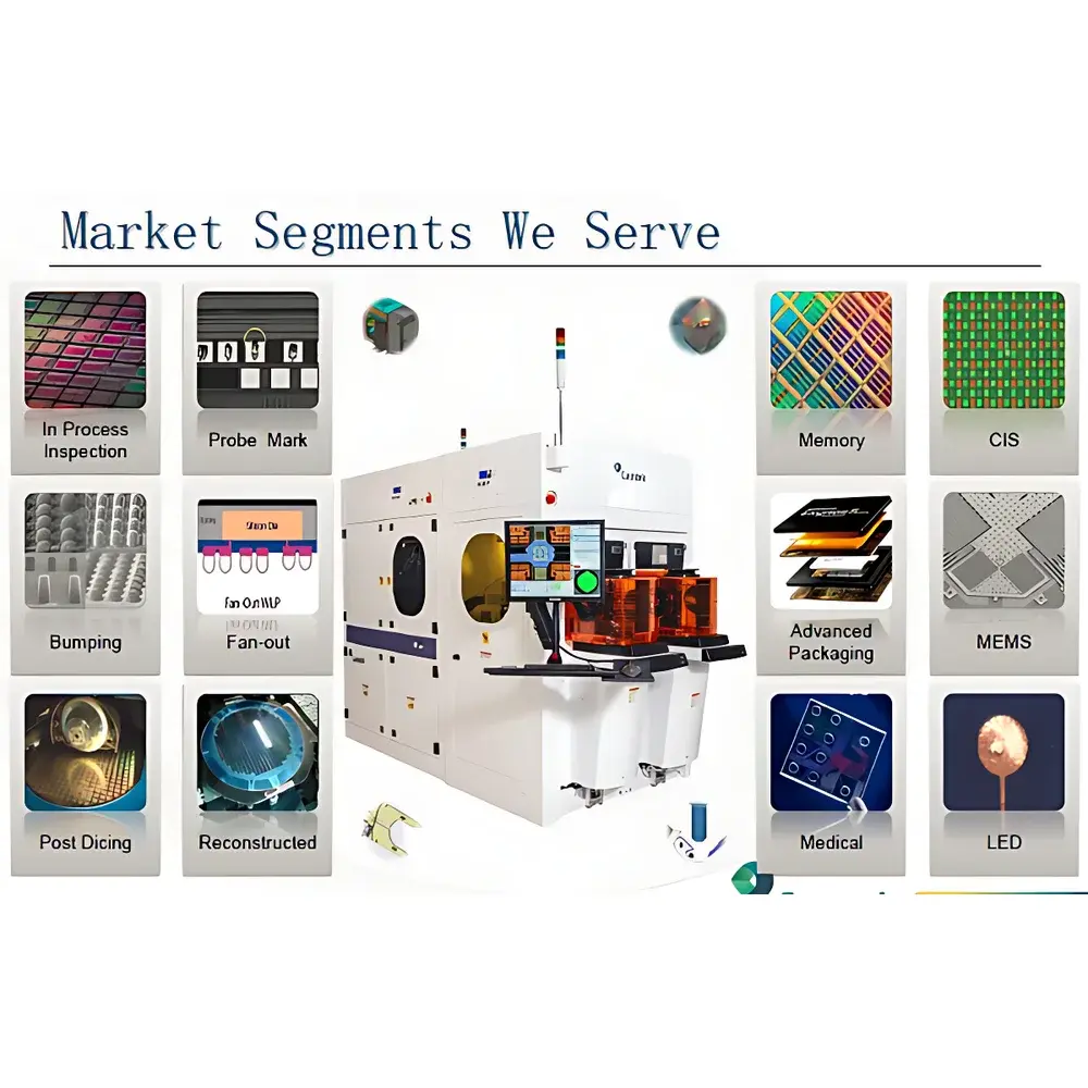
Applications
- Wafer-level bump inspection pre- and post-reflow: coplanarity, diameter, shape deviation, bridging, missing bumps
- RDL metrology: line width/spacing uniformity, edge roughness (LWR), open/short detection on sub-2 µm features
- TSV fill characterization: void detection, step coverage quantification, recess depth profiling
- CMOS image sensor array validation: microlens alignment, color filter integrity, pixel-level defect grading
- MEMS device structural verification: movable comb-finger spacing, cavity depth, stiction assessment
- LED epitaxial wafer inspection: pit density, scratch mapping, epi-layer thickness variation (via interference fringe analysis)
- OQC final release testing for fan-out wafer-level packaging (FOWLP) and 2.5D/3D IC integration substrates
FAQ
What wafer sizes and materials does the Eagle-I Series support?
The system supports 150 mm, 200 mm, and 300 mm wafers made of silicon, SiC, GaAs, glass, and organic laminates — including thinned, warped, and temporarily bonded substrates.
Is the system compatible with existing fab automation infrastructure?
Yes — it features full SECS/GEM and PV2 communication stacks, supports host-directed job dispatch, and provides real-time equipment status reporting via HSMS.
How is measurement traceability ensured for quality audits?
All calibration events, software revisions, and operator actions are logged with timestamps and digital signatures in accordance with ISO/IEC 17025 and FDA 21 CFR Part 11 requirements.
Can the Eagle-AP perform true 3D profilometry, or is it limited to height estimation?
The Eagle-AP employs focus-variation-based 3D reconstruction validated against NIST-traceable step-height standards, delivering quantitative topography with ≤0.05 µm repeatability over 100 µm vertical range.
Does the system support machine learning–based defect classification?
While the base platform uses deterministic rule-based classification, optional AI-assisted review modules (Inspector™ ML) are available for supervised training on customer-specific defect signatures — deployed as containerized inference engines meeting ITAR and GDPR data residency requirements.
Related Products


