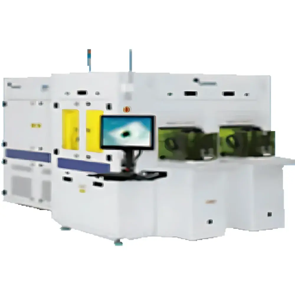
CAMTEK EagleT-i Advanced 2D Automatic Optical Inspection System
| Origin | Imported |
|---|---|
| Manufacturer Type | Authorized Distributor |
| Model | EagleT-i |
| Price Range | USD 650,000 – 1,050,000 |
| Inspection Speed | Up to 50 million bump measurement points per wafer |
| 2D Detection Accuracy | 0.2 µm |
| 3D Height Measurement Accuracy | 0.05 µm (Measurement Range: 2–100 µm) |
| Minimum Detectable Line Width/Spacing | 2 µm (post-RDL) |
| Defect Detection Limit | 0.2 µm surface anomalies |
| Compatible Substrates | Flat and warped wafers, square dies, compound semiconductor substrates |
Overview
The CAMTEK EagleT-i is a high-throughput, high-precision 2D automatic optical inspection (AOI) system engineered specifically for advanced semiconductor packaging and front-end-of-line (FEOL) process control. Utilizing a multi-spectral, high-resolution imaging architecture coupled with real-time pixel-level image acquisition and proprietary sub-pixel alignment algorithms, the EagleT-i performs non-contact, high-magnification surface inspection and critical dimension (CD) metrology on patterned wafers and bare dies. Its core detection methodology relies on calibrated bright-field/dark-field illumination, telecentric optics, and adaptive focus stacking — enabling robust defect classification (e.g., bridging, missing bumps, micro-scratches, residue, misalignment) and quantitative geometric analysis without physical contact or sample preparation. Designed for integration into high-volume manufacturing (HVM) environments, the EagleT-i meets the stringent repeatability and traceability requirements of semiconductor fab qualification protocols.
Key Features
- Ultra-high-speed inspection engine capable of acquiring and processing >50 million bump measurement points per full 300 mm wafer in under 90 seconds — optimized for post-plating, post-RDL, and post-dicing process steps.
- Sub-0.2 µm 2D spatial resolution supported by precision air-bearing XY stage, active vibration isolation, and thermally stabilized optical path — certified per ISO 10110-5 and SEMI E10 standards.
- Dual-mode imaging platform: simultaneous high-SNR 2D intensity mapping and edge-enhanced contrast imaging via patented RealSharp™ image sharpening technology — eliminating motion blur and preserving sub-micron feature fidelity at full frame rate.
- CAD-based template matching with hierarchical layer registration: supports GDSII/OASIS import, automated die-to-die and die-to-database comparison, and configurable tolerance bands per feature class (e.g., bump diameter ±0.3 µm, pitch deviation ±0.15 µm).
- Flexible substrate handling: accommodates standard round wafers (150–300 mm), square dies (up to 120 × 120 mm), and warped substrates up to 3 mm bow — equipped with vacuum-assisted chuck and real-time topography compensation.
- Modular optical configuration: interchangeable objectives (5×–100×), motorized zoom, and multi-angle LED illumination arrays enable application-specific optimization for Cu pillar, NiAu bump, RDL trace, TSV opening, and MEMS cavity inspection.
Sample Compatibility & Compliance
The EagleT-i is validated for use across compound semiconductor and silicon-based platforms including CMOS image sensors, MEMS inertial devices, GaN-based LEDs, and 2.5D/3D IC interposers. It supports inspection of bump metallurgies (SnAg, CuNiSn, Au stud), redistribution layers (polyimide, BCB, SiO₂), and ultra-fine-pitch structures down to 2 µm line width/spacing. All hardware and software components comply with SEMI S2/S8 safety and environmental specifications. The system’s calibration traceability is maintained through NIST-traceable step-height standards and certified reference wafers (e.g., NIST SRM 2056, VLSI Standards WAF-100). For regulated production environments, optional audit trail logging, electronic signature support, and user access controls align with FDA 21 CFR Part 11 and ISO 9001/14001 quality management frameworks.
Software & Data Management
Powered by CAMTEK’s proprietary InspectorX™ software suite, the EagleT-i delivers integrated defect review, statistical process control (SPC), and yield analytics. The software features a fully scriptable API (Python/C++), real-time dashboarding with OEE metrics, and native integration with factory host systems via SECS/GEM and MQTT protocols. Defect data is stored in a relational database compliant with SQL-92 standards, supporting automated root cause correlation across process tools (e.g., plating current density, litho exposure dose, etch uniformity). All image archives are preserved in lossless TIFF-6.0 format with embedded EXIF metadata (timestamp, lens ID, focus Z-position, illumination settings). Optional modules include AI-assisted defect classification (trained on >2.7 million labeled bump images), automated bin-map generation for probe station handoff, and cross-tool yield prediction using multivariate regression models.
Applications
- Post-electroplating bump inspection: quantification of coplanarity, diameter distribution, and void detection in SnAg and CuNiSn micro-bumps (25–150 µm pitch).
- RDL metrology: line width/spacing verification, edge roughness (LWR/LER) assessment, and dielectric coverage uniformity on polyimide or BCB layers.
- TSV fill inspection: via opening detection, aspect ratio validation, and copper overburden height mapping pre-CMP.
- MEMS cavity integrity: identification of particulate contamination, membrane deformation, and seal ring continuity in pressure sensor and microphone dies.
- OQC final wafer screening: comprehensive defect grading per JEDEC JESD22-A108 and AEC-Q200 automotive reliability criteria.
- CMOS image sensor pixel array verification: hot pixel cluster detection, microlens alignment error quantification, and color filter array (CFA) registration accuracy.
FAQ
What wafer sizes and form factors does the EagleT-i support?
The system handles 150 mm, 200 mm, and 300 mm silicon wafers, as well as square dies up to 120 × 120 mm and compound semiconductor substrates (e.g., sapphire, SiC). Warped wafers with total indicator reading (TIR) up to 3 mm are accommodated via dynamic Z-focus compensation.
Does the EagleT-i provide both 2D and 3D measurement capabilities?
The EagleT-i is a dedicated 2D AOI platform. For combined 2D/3D functionality, CAMTEK offers the EagleAP platform — which integrates confocal chromatic sensing and structured light profilometry alongside the same optical inspection engine.
How is measurement accuracy verified and maintained?
Calibration is performed using NIST-traceable step-height standards and certified photomask reference wafers. Daily automated self-check routines validate stage positioning repeatability (<±15 nm), optical magnification stability (±0.01%), and illumination uniformity (±1.2% across FOV). Full recalibration is recommended every 12 months or after major maintenance.
Can the EagleT-i integrate with existing MES or SPC systems?
Yes — native SECS/GEM communication, OPC UA server, and RESTful API enable seamless bidirectional data exchange with leading MES (Applied Materials EnduraLink, PDF Solutions Exensio) and SPC platforms (InfinityQS ProFicient, Minitab Engage).
Is CAD-based inspection supported for custom package layouts?
Absolutely. InspectorX™ accepts GDSII, OASIS, and DXF inputs. Layer alignment is achieved via fiducial-based registration with sub-50 nm overlay accuracy, and rule-based inspection recipes can be generated automatically from design hierarchy and DRC rule decks.
Related Products


