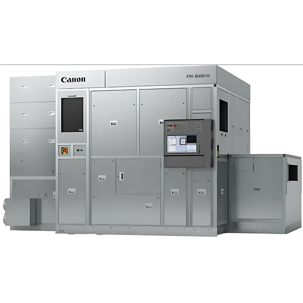


Canon FPA-8000iW / FPA-8000AS / FPA-3000EX6 / FPA-5520iV / FPA-1200NZ2C Mask Aligner & Projection Stepper Systems
| Brand | Canon (Japan) |
|---|---|
| Origin | Japan |
| Equipment Type | Mask Lithography System (Stepper/Scanner/NIL) |
| Wafer/Substrate Compatibility | 200 mm, 300 mm, Gen 8.6 to Gen 10.5 FPD glass |
| Resolution | ≤65 nm (KrF stepper, with multi-patterning), 0.18–0.35 µm (i-line/KrF), 1–2 µm (packaging), 3–5 µm (FPD), <10 nm (NIL, theoretical) |
| Exposure Source | i-line (365 nm), KrF (248 nm), NIL UV imprint |
| Alignment Accuracy | ±0.5 µm (FPA-5520iV) |
| Throughput | ~100–120 wph (300 mm, FPA-8000 series) |
| Compliance | ISO 14644-1 Class 5 cleanroom compatible, SEMI S2/S8 certified, supports GLP/GMP-aligned process documentation |
Overview
Canon’s mask lithography systems—comprising steppers, scanners, and nanoimprint lithography (NIL) platforms—are engineered for high-precision pattern transfer in semiconductor front-end, advanced packaging, flat-panel display (FPD), and MEMS manufacturing. Unlike EUV-based scanners, Canon’s optical lithography tools rely on mature deep-ultraviolet (DUV) sources—including i-line (365 nm) and KrF excimer (248 nm)—combined with high-numerical-aperture projection optics and precision wafer-stage metrology. These systems operate on the principle of contact, proximity, or reduction projection exposure, where a photomask defines the circuit pattern transferred onto photoresist-coated substrates via controlled UV irradiation. While Canon does not compete in sub-7 nm logic node production, its platforms deliver robust performance in mature-node IC fabrication (≥65 nm), fan-out wafer-level packaging (FO-WLP), through-silicon via (TSV) patterning, and high-resolution OLED/LCD backplane manufacturing—applications demanding repeatability, thermal stability, and long-term tool uptime rather than extreme resolution alone.
Key Features
- Modular platform architecture supporting multiple exposure modes: step-and-repeat (stepper), step-and-scan (scanner), and UV nanoimprint lithography (NIL)
- Integrated laser interferometry-based stage positioning with sub-100 nm overlay accuracy and real-time dynamic focus control
- Dual-wavelength illumination options (i-line and KrF) with automated spectral calibration and dose uniformity compensation
- Advanced mask alignment subsystem featuring CCD-based image recognition, multi-point fiducial detection, and automatic rotational correction (±0.001°)
- Thermally stable granite base and vacuum-chuck substrate handling to minimize thermal drift during extended exposure sequences
- Robust mechanical design compliant with SEMI S2 (safety) and S8 (ergonomics) standards; CE-marked and UL-listed for global deployment
Sample Compatibility & Compliance
Canon lithography systems accommodate a broad range of substrate formats: silicon wafers (200 mm and 300 mm), quartz masks, fused silica reticles, and large-area glass substrates up to Gen 10.5 (2940 × 3370 mm). The FPA-5520iV and FPA-3030iWa are optimized for bump patterning and redistribution layer (RDL) formation in flip-chip and 2.5D/3D integration processes, while the MPA-8000 series supports high-throughput TFT array exposure for AMOLED and microLED displays. All systems comply with ISO 14644-1 Class 5 cleanroom operational requirements. Process data logging, user access control, and audit trail functionality align with FDA 21 CFR Part 11 and EU Annex 11 expectations for regulated environments—enabling traceable, validated lithography workflows in GMP-compliant packaging fabs and display pilot lines.
Software & Data Management
Canon’s proprietary LITHO-OS software suite provides unified control across exposure, alignment, focus, and dose modules. It supports recipe-driven operation with version-controlled parameter sets, in-situ CD monitoring via integrated metrology feedback loops, and automated defect-aware exposure sequencing. Data export conforms to SECS/GEM and STDF standards for seamless integration into factory automation (FA) systems. Full audit trail logging—including operator ID, timestamp, parameter changes, and error codes—is retained for ≥12 months and exportable in CSV/PDF format. Optional software modules enable DOE-based process window analysis, multi-layer overlay modeling, and statistical process control (SPC) charting per JEDEC JESD22-A114 guidelines.
Applications
- Mature-node IC fabrication: analog, power management, automotive MCUs (65–180 nm nodes using KrF/i-line with double-patterning)
- Advanced packaging: RDL, bump, TSV, and interposer patterning with ≤2 µm resolution and ±0.5 µm overlay accuracy
- Flat-panel display manufacturing: high-uniformity TFT backplane exposure on Gen 8.6–Gen 10.5 glass substrates
- MEMS and sensor fabrication: high-aspect-ratio structure definition on SOI and compound semiconductors
- NAND flash and photonic integrated circuit (PIC) prototyping using FPA-1200NZ2C NIL platform (sub-10 nm feature replication without complex optics)
FAQ
Does Canon offer EUV lithography systems?
No. Canon does not develop or commercialize extreme ultraviolet (EUV) lithography tools. Its DUV portfolio centers on i-line and KrF exposure technologies, supplemented by nanoimprint lithography as an alternative path for sub-10 nm patterning.
Can Canon steppers support 300 mm wafer processing?
Yes. The FPA-8000 series is fully qualified for 300 mm (12-inch) silicon wafers, including automated cassette-to-cassette loading and edge exclusion mapping.
Is NIL technology from Canon suitable for high-volume manufacturing?
The FPA-1200NZ2C NIL system is deployed in R&D and low-to-medium volume production (e.g., NAND patterning, photonic devices), but throughput remains lower than optical steppers. Mass adoption awaits further improvements in template lifetime, defect mitigation, and resist compatibility.
What metrology standards do Canon lithography systems reference?
Overlay accuracy is verified per SEMI E10 (Specification of Definition and Measurement of Equipment Reliability), while critical dimension uniformity follows SEMI E142 (CD Uniformity Measurement Standard). Calibration protocols align with NIST-traceable interferometric references.
Are Canon lithography tools compatible with industry-standard photomasks?
Yes. All systems accept standard quartz/chrome binary masks and phase-shift masks (PSM) with standard reticle frames (e.g., SEMI MS7, MS12), including pellicle-integrated configurations.


