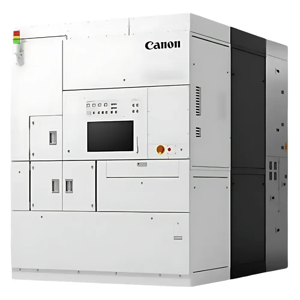
Canon FPA5000 ES4 Scanning Stepper Lithography System
| Brand | Canon |
|---|---|
| Origin | Japan |
| Manufacturer Type | Authorized Distributor |
| Product Origin | Imported |
| Model | FPA5000 ES4 |
| Resolution | 0.13 µm |
| Exposure Wavelength | 248 nm |
| Maximum Exposure Field | 26 mm × 33 mm |
| Numerical Aperture (NA) | 0.5–0.8 |
| Reduction Ratio | 4:1 |
| Overlay Accuracy | ±25 nm |
Overview
The Canon FPA5000 ES4 is a high-precision scanning stepper lithography system engineered for advanced microfabrication in non-standard semiconductor and microdevice manufacturing environments. Unlike conventional projection steppers that rely on step-and-repeat exposure, the FPA5000 ES4 employs a synchronized scanning mechanism—where both mask and wafer move continuously under controlled velocity and phase alignment—to achieve superior resolution and dose uniformity across large exposure fields. Operating at a deep ultraviolet (DUV) wavelength of 248 nm (KrF excimer laser), the system delivers sub-130 nm half-pitch resolution (≤0.13 µm) with a 4:1 reduction optical train and an adjustable numerical aperture (NA) range of 0.5 to 0.8. Designed for flexibility beyond mainstream logic and memory fabs, it supports 150 mm (6″), 200 mm (8″), and 300 mm (12″) wafers and is widely deployed in compound semiconductor R&D, MEMS prototyping, LED epitaxial patterning, and specialty sensor fabrication.
Key Features
- Scanning stepper architecture enabling high-resolution patterning with enhanced depth-of-focus control compared to static exposure systems
- Dedicated KrF excimer laser illumination source (248 nm) with integrated spectral bandwidth narrowing and energy stabilization
- Optimized telecentric projection optics with 4:1 reduction ratio and NA tunability (0.5–0.8) for trade-off optimization between resolution, depth of focus, and process latitude
- Maximum exposure field of 26 mm × 33 mm—suitable for full-chip or multi-die exposures on non-standard substrates including SiC, GaN, sapphire, and quartz
- Sub-25 nm overlay accuracy (3σ) enabled by interferometric stage metrology, real-time wafer alignment feedback, and thermal drift compensation algorithms
- Modular platform design supporting integration with automated track systems, vacuum chucks, and backside alignment modules for opaque or warped substrates
Sample Compatibility & Compliance
The FPA5000 ES4 accommodates a broad spectrum of substrate types and thicknesses, including silicon, SOI, GaAs, InP, SiC, sapphire, fused silica, and flexible polymer films (e.g., PI or PET) when mounted on compatible carriers. It complies with SEMI S2/S8 safety standards and meets electromagnetic compatibility (EMC) requirements per IEC 61000-6-3/6-4. The system’s motion control and exposure sequencing are designed to support GLP-compliant process documentation workflows, and its software architecture permits audit-trail logging aligned with FDA 21 CFR Part 11 principles where integrated with validated host systems. While not certified for high-volume manufacturing (HVM) in logic foundries, it satisfies ISO 9001-aligned qualification protocols for pilot-line and low-to-medium volume production in compound semiconductor and MEMS facilities.
Software & Data Management
Controlled via Canon’s proprietary LITHO-MASTER™ platform, the FPA5000 ES4 provides hierarchical recipe management, multi-layer alignment calibration routines, and real-time exposure dose monitoring with closed-loop feedback. All operational parameters—including stage position, lens focus offset, reticle temperature, and laser pulse energy—are logged with timestamped metadata in standardized ASCII-based log formats. Export capabilities include GDSII-compatible pattern data ingestion, CD-SEM correlation reports, and overlay error decomposition (X/Y translation, rotation, magnification, orthogonality). Data retention policies and user access controls can be configured to align with internal IT security frameworks or external regulatory review requirements.
Applications
- Compound semiconductor device fabrication: HEMT gate patterning on GaN-on-Si, VCSEL mesa definition on InP, and RF filter structures on LiNbO₃
- MEMS development: High-aspect-ratio comb drives, inertial sensor proof masses, and microfluidic channel networks requiring critical dimension control below 150 nm
- Micro-LED and mini-LED manufacturing: Pixel-level patterning on sapphire or GaN templates with strict registration tolerance across heterogeneous substrates
- Photonic integrated circuit (PIC) prototyping: Grating coupler arrays, waveguide bends, and modulator electrodes demanding sub-100 nm edge placement accuracy
- Research-grade maskless lithography evaluation: Used as a reference tool for benchmarking direct-write systems (e.g., e-beam or DUV laser writers) in university cleanrooms and national labs
FAQ
What wafer sizes does the FPA5000 ES4 support?
The system is configured for 150 mm (6″), 200 mm (8″), and 300 mm (12″) wafers, with optional adaptors available for non-circular or irregular substrates up to 33 mm × 26 mm in active exposure area.
Is the 248 nm illumination source internally integrated or externally coupled?
The KrF excimer laser is fully integrated within the illumination column, including beam homogenization optics, attenuators, and pulse energy monitoring sensors—no external laser coupling is required.
Can the FPA5000 ES4 perform backside alignment?
Yes, with optional backside alignment module (BSA-ES4), the system supports infrared-based through-wafer alignment for opaque substrates such as SiC or metal-coated wafers.
Does Canon provide process qualification support for new resist materials?
Canon offers application engineering services—including resist sensitivity mapping, PAG optimization, and post-exposure bake (PEB) profiling—for qualified photoresists used in DUV lithography, subject to NDA and joint development agreements.
What level of maintenance training is available for end users?
Canon-certified technicians deliver on-site operator and maintenance training covering daily calibration, alignment verification, preventive maintenance schedules, and basic fault diagnostics—aligned with SEMI E10 equipment reliability guidelines.


