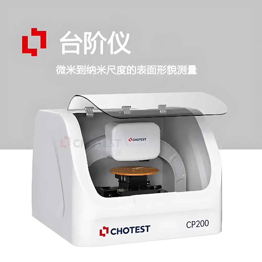
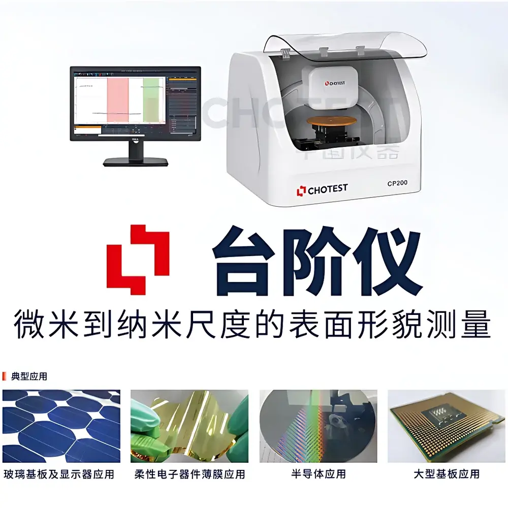
Chotest NS Series Step Height Measurement Instrument (LVDC Contact Profilometer)
| Brand | Chotest |
|---|---|
| Origin | Guangdong, China |
| Manufacturer Type | Authorized Distributor |
| Country of Origin | China |
| Model | NS200 |
| Price | USD 84,000 (FOB Shenzhen) |
| Measurement Principle | Linear Variable Differential Capacitance (LVDC) |
| Probe Tip Radius | 2 µm |
| Scan Length | 55 mm |
| Step Height Repeatability | 0.5 Å (at 330 µm range) |
| Vertical Resolution | Sub-Ångström |
| Force Range | 1–50 mg (adjustable, closed-loop micro-electromagnetic control) |
| XY Stage | Motorized, 150 mm × 150 mm |
| Rotation Stage | 360° motorized |
| Z-Axis Lift | Motorized |
| Optical Navigation | 5 MP color camera, FOV 2200 × 1700 µm |
| Max Sample Thickness | 50 mm |
| Wafer Compatibility | 150 mm (6″) and 200 mm (8″) |
| Operating Environment | 16–25 °C, ΔT < 2 °C/h, RH 30–40 % (non-condensing), Vibration ≤ 6.35 µm/s (1–100 Hz), Acoustic Noise ≤ 80 dB, Airflow ≤ 0.508 m/s downward |
Overview
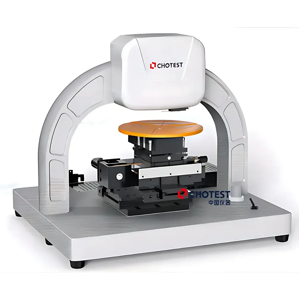
The Chotest NS Series Step Height Measurement Instrument is a high-precision, contact-mode surface profilometer engineered for sub-nanometer vertical metrology in R&D and production environments. It employs a Linear Variable Differential Capacitance (LVDC) displacement sensor—distinct from optical interferometry or stylus-based inductive systems—to deliver true sub-Ångström resolution (≤ 0.5 Å at 330 µm vertical range) with exceptional long-term stability. The LVDC principle relies on capacitance variation between a fixed reference electrode and a movable probe tip, enabling direct, drift-free displacement transduction without mechanical hysteresis or thermal expansion artifacts common in piezoresistive or strain-gauge systems. Designed around a monolithic single-arch龙门 (gantry) architecture, the instrument minimizes environmental coupling—particularly acoustic and floor-borne vibration—ensuring measurement integrity in standard cleanroom or lab settings compliant with ISO 25178-601 and ASTM E2927-22 guidelines for areal surface texture measurement. Its core application domain spans thin-film metrology, process validation in semiconductor front-end and back-end fabrication, MEMS release etch characterization, and optical coating thickness verification where non-destructive, traceable, and NIST-traceable step height data is required.
Key Features
- Sub-Ångström vertical resolution enabled by ultra-low-noise LVDC sensor electronics and real-time digital feedback compensation
- Programmable probe force (1–50 mg) via low-inertia electromagnetic actuation—preserving surface integrity on soft polymers, photoresists, and fragile dielectric stacks while maintaining stable contact on hard SiO₂ or sapphire substrates
- Integrated 5-megapixel color navigation camera with calibrated field-of-view (2200 × 1700 µm) and real-time overlay of scan trajectory onto live optical image—enabling precise feature targeting without manual alignment
- Motorized 3-axis stage system: X/Y translation (150 mm × 150 mm), full 360° programmable rotation, and precision Z-lift—supporting automated multi-site measurement across wafers, masks, and irregularly shaped substrates
- Single-pass scan length of 55 mm with straightness error < 50 nm over full travel—achieved via air-bearing-equivalent linear guides and active motion profile optimization to suppress velocity-induced contour distortion
- Thermal and mechanical isolation design: base plate with constrained-layer damping, internal temperature stabilization (±0.1 °C), and passive vibration attenuation meeting SEMI S2/S8 requirements
Sample Compatibility & Compliance
The NS200 imposes no material-specific constraints on reflectivity, conductivity, or hardness—making it suitable for opaque, transparent, conductive, insulating, or viscoelastic surfaces. It routinely measures ITO, SiNₓ, Al₂O₃, SU-8, PDMS, and metal-dielectric multilayers without signal saturation or tip wear. All measurements adhere to ISO 25178-2 (areal surface texture parameters), ISO 4287 (profile roughness), and ASTM E1316 (nondestructive evaluation terminology). Data acquisition and reporting modules support audit trails compliant with FDA 21 CFR Part 11 (electronic records/signatures), including user authentication, parameter locking, and immutable measurement log export (CSV, XML, HDF5). Calibration certificates are issued per ISO/IEC 17025-accredited procedures, with traceability to PTB (Physikalisch-Technische Bundesanstalt) reference standards.
Software & Data Management
The proprietary Chotest ProfilerSuite v4.2 software provides full instrument control, real-time visualization, and ISO-compliant parameter extraction. It supports custom scripting (Python API) for integration into automated test sequences and MES/SCADA environments. Key capabilities include:
- Smart path planning using hybrid coordinate input: absolute stage coordinates, relative offsets, or image-based landmark recognition
- Automated multi-region measurement—defining up to 128 sites per wafer with conditional logic (e.g., “measure only if RMS < 0.8 nm”)
- SPC dashboard with X-bar/R charts, Cpk/Ppk calculation, trend analysis, and alarm thresholds aligned with JIS Z 9021 and AIAG SPC manuals
- Batch report generation with embedded calibration metadata, environmental logs, and operator ID—exportable as PDF/A-1b or structured XML for LIMS ingestion
- GLP/GMP mode: enforced electronic signatures, revision-controlled method templates, and automatic backup to network-attached storage with SHA-256 hash verification
Applications
The NS200 delivers quantitative surface topography data critical for process development and quality assurance across multiple advanced manufacturing sectors:
- Semiconductor: Quantifying film thickness loss/gain after CMP, etch uniformity mapping on 300 mm wafers, gate oxide step coverage analysis, and TSV depth profiling
- Photovoltaics: Measuring anti-reflective coating thickness on textured silicon, passivation layer uniformity on PERC cells, and laser ablation trench depth
- Optics & Photonics: Characterizing multilayer dielectric stack steps on AR/HR coatings, lens mold surface fidelity, and grating groove depth consistency
- MEMS & NEMS: Validating release etch depth, cantilever undercut geometry, and stiction-related deformation post-packaging
- Academic research: In-situ monitoring of atomic layer deposition growth rates, polymer brush swelling kinetics, and 2D material transfer layer thickness
FAQ
What is the minimum measurable step height with guaranteed repeatability?
The NS200 achieves ≤ 0.5 Å (0.05 nm) repeatability for steps ≥ 1 µm in height under controlled environmental conditions (ISO Class 5 cleanroom, stabilized temperature). For sub-10 nm steps, repeatability is specified at ±1.0 Å (1σ) per ASTM E2927 Annex A3.
Does the system require periodic recalibration against physical step standards?
Yes—annual calibration is recommended using NIST-traceable step height standards (e.g., NIST SRM 2160a). The instrument includes built-in self-diagnostic routines that monitor sensor linearity, stage orthogonality, and thermal drift compensation performance.
Can the NS200 measure on curved or tilted substrates?
Yes—through combined use of the motorized tilt stage (±5°), 360° rotation, and software-based local plane fitting algorithms. Surface tilt up to ±3° is automatically compensated during scanning; beyond that, iterative leveling routines are supported.
Is the software compatible with Windows 11 and 64-bit architectures?
ProfilerSuite v4.2 supports Windows 10/11 (64-bit), requires .NET Framework 4.8, and is validated on Intel Core i7-10xxx or AMD Ryzen 7 5800X platforms with ≥ 32 GB RAM and dedicated GPU (NVIDIA Quadro P2000 or equivalent).
What documentation is provided for regulatory submissions (e.g., FDA, CE)?
A complete Technical File Package—including Design History File (DHF) excerpts, Risk Management Report (ISO 14971), Electromagnetic Compatibility (EMC) test reports (EN 61326-1), and Software Validation Protocol (per IEC 62304)—is available upon request for qualified customers under NDA.