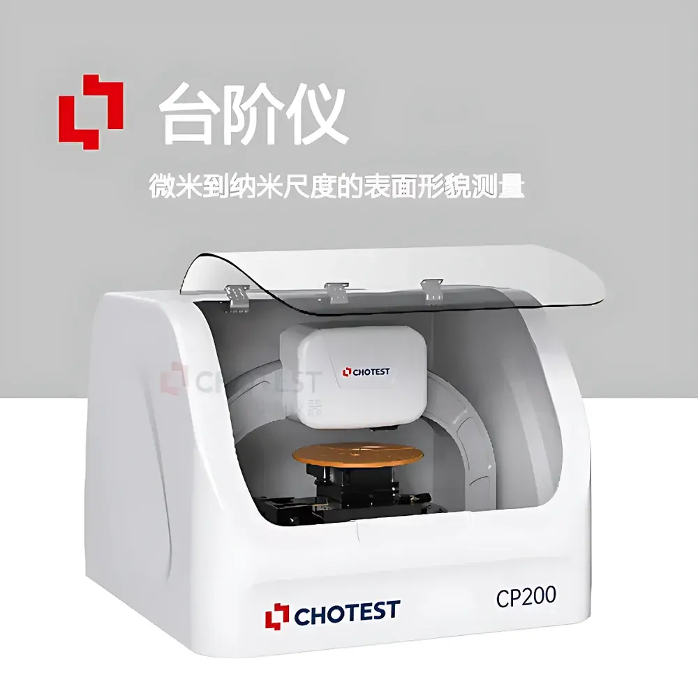
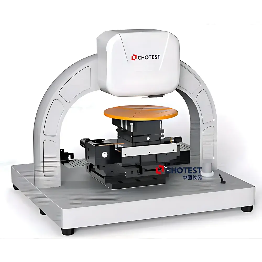
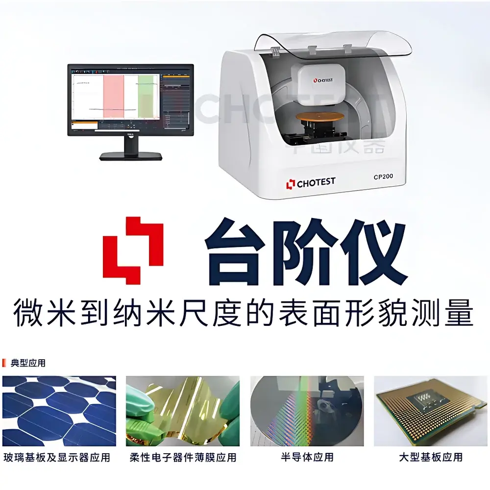
Chotest NS200 Probe-Based Nanoscale Surface Profilometer
| Brand | Chotest |
|---|---|
| Origin | Guangdong, China |
| Manufacturer Type | Authorized Distributor |
| Country of Origin | China |
| Model | NS200 |
| Price | USD 84,000 (FOB) |
| Measurement Principle | Capacitive (LVDC) |
| XY Stage Travel | 150 mm × 150 mm |
| Maximum Scan Length | 55 mm |
| Step Height Repeatability | ±0.005 nm (5 Å) |
| Max Sample Size | 200 mm (8-inch wafer) |
| Sensor Resolution | 0.01 Å (sub-angstrom) at 13 µm range |
| Force Control | Adjustable from 1 µN to 10 mN |
| Vertical Range | 13 µm (standard), optional up to 1050 µm |
| Optical Navigation | 5 MP color camera (orthogonal or oblique view) |
| SPC Module | Yes |
| Environmental Requirements | 16–25 °C, ≤40% RH (non-condensing), vibration <6.35 µm/s (1–100 Hz) |
Overview
The Chotest NS200 is a high-precision, contact-mode surface profilometer engineered for nanoscale topographic characterization of microstructured surfaces. It operates on the principle of capacitive displacement sensing—specifically, Linear Variable Differential Capacitance (LVDC)—to convert vertical probe deflection into sub-angstrom-resolved electrical signals. Unlike optical interferometric or confocal methods, the NS200 delivers direct traceable height metrology without dependence on surface reflectivity, material transparency, or optical contrast. Its core application domain includes quantitative measurement of step heights, thin-film thicknesses, surface roughness (Ra, Rq, Rz, Rp, Rv), waviness, and thin-film stress—critical parameters in semiconductor fabrication (e.g., etch depth monitoring, CMP endpoint detection), MEMS development, photomask QA, and advanced coating R&D. The instrument integrates a rigid single-arch龙门 (gantry) mechanical architecture with ultra-low-inertia probe actuation, enabling stable, low-noise scanning across both hard substrates (Si, SiO₂, sapphire) and compliant materials (polymers, photoresists, biological films).
Key Features
- Sub-angstrom resolution LVDC sensor (0.01 Å at 13 µm full scale) with <0.02% linearity error and SNR >100 dB, enabling reliable quantification of features from <1 nm to >1 mm in vertical scale.
- Adjustable probing force (1 µN – 10 mN) via electromagnetic actuation—ensuring non-destructive contact on soft polymers while maintaining stability on brittle oxides or nitrides.
- Motorized XYZ stage with 150 mm × 150 mm travel, integrated 360° continuous-rotation θ-stage, and sub-micron positioning repeatability (<±100 nm) for precise alignment of complex geometries and off-axis structures.
- Dual-mode optical navigation: 5 MP color camera supports orthogonal-view sample framing and oblique-view real-time scan-track overlay—enabling accurate placement of scan paths within ±1 µm spatial tolerance.
- Magnetic quick-change probe mount with automated software-guided recalibration—reducing downtime during tip replacement and ensuring consistent tip radius (2 µm diamond standard) traceability per ISO 25178-602.
- Active vibration isolation platform and acoustic enclosure compliant with ISO 20483 Class A environmental specifications—maintaining measurement integrity under typical lab conditions (≤6.35 µm/s floor vibration, ≤80 dB ambient noise).
Sample Compatibility & Compliance
The NS200 imposes no intrinsic restrictions on sample material class, optical properties, or surface hardness. It accommodates wafers up to 200 mm (8-inch), substrates up to 50 mm thick, and irregularly shaped components mounted on custom fixtures. Surface reflectivity, absorption coefficient, or dielectric constant do not affect measurement fidelity—making it suitable for opaque metals, transparent glasses, low-k dielectrics, and organic thin films alike. The system complies with key international standards for surface texture metrology: ISO 25178-2 (areal surface texture parameters), ISO 4287 (profile-based roughness), ASTM E1393 (step height calibration), and ISO/IEC 17025 requirements for accredited calibration laboratories. Data acquisition and reporting modules support audit-ready traceability aligned with GLP and GMP workflows—including electronic signatures, version-controlled SOPs, and 21 CFR Part 11–compliant audit trails when deployed with optional secure software licensing.
Software & Data Management
The proprietary Chotest ProfilSoft™ platform provides modular, workflow-driven operation. Core modules include: Auto-Focus & Navigation Assistant (AFA), Multi-Region Batch Scan Scheduler, 3D Surface Reconstruction Engine (with mesh smoothing and interpolation filters), SPC Dashboard (X̄-R charts, Cp/Cpk calculation, trend analysis across ≥1000 data points), and Export-Ready Reporting (PDF, CSV, STEP, STL). All raw sensor data are stored in HDF5 format with embedded metadata (timestamp, operator ID, environmental logs, calibration certificate IDs). Software supports scripting via Python API for integration into automated fab metrology lines or AI-driven defect classification pipelines. Calibration certificates—including tip radius verification, stage linearity mapping, and sensor drift compensation—are digitally signed and archived with SHA-256 checksums.
Applications
- Semiconductor process control: Quantifying trench depth uniformity post-RIE, measuring film thickness loss during wet etch, validating CMP planarity (within-wafer non-uniformity <0.5%), and characterizing STI step coverage.
- MEMS/NEMS device metrology: Measuring comb-drive gap heights, cantilever curvature, and release etch undercut profiles with <1 nm repeatability.
- Optical component QA: Verifying anti-reflective coating step edges, diffractive optical element (DOE) groove depth consistency, and laser mirror substrate flatness deviations.
- Advanced packaging: Characterizing copper pillar height variation, under-bump metallization (UBM) topography, and mold compound planarization after grinding.
- Academic & national metrology labs: Serving as a reference instrument for step-height artifact certification (NIST-traceable SRMs), inter-laboratory comparison studies, and development of new surface parameter definitions per ISO TC213 working groups.
FAQ
What is the minimum measurable step height with guaranteed repeatability?
The NS200 achieves ±0.005 nm (5 Å) repeatability for steps ≥1 nm in height, verified using NIST SRM 2159 silicon grating artifacts under controlled environmental conditions.
Can the system measure steep sidewalls or high-aspect-ratio features?
Yes—the 2 µm radius diamond stylus supports sidewall angles up to 75°; optional conical tips (1 µm apex) extend capability to >85°, subject to tip wear monitoring and recalibration.
Is thermal drift compensated during long-duration scans?
Yes—real-time temperature monitoring (±0.1 °C) feeds into a dynamic offset correction algorithm that adjusts baseline position every 10 seconds during scans >60 s.
Does the software support automated pass/fail judgment against user-defined tolerances?
Yes—threshold-based rule engines allow defining multi-parameter acceptance criteria (e.g., “Rz < 2.5 nm AND step height = 125.0 ± 0.8 nm”) with auto-flagging and PDF report generation.
What calibration standards are recommended for routine verification?
Chotest recommends annual verification using ISO 5436-1 step-height standards (e.g., PTB U50 series) and quarterly tip radius checks via SEM imaging per ISO 25178-602 Annex B.