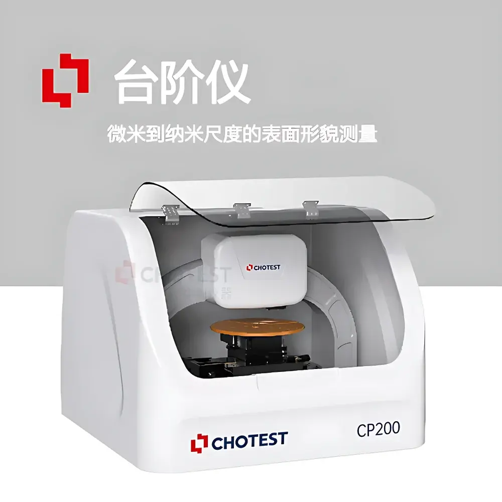
Chotest NS200 Stylus Profilometer for Thin-Film Step Height and Surface Topography Measurement
| Brand | Chotest |
|---|---|
| Origin | Guangdong, China |
| Manufacturer Type | Authorized Distributor |
| Country of Origin | China |
| Model | NS200 |
| Price | USD 84,000 (FOB Shenzhen) |
| Measurement Principle | Contact-mode stylus profilometry with LVDC capacitive transduction |
| Vertical Resolution | Sub-ångström (≤0.1 Å) |
| Lateral Scan Range | 55 mm |
| X/Y Stage Travel | 150 mm × 150 mm (motorized) |
| R-θ Stage | 360° continuous motorized rotation |
| Max Sample Thickness | 50 mm |
| Wafer Compatibility | 150 mm (6″) and 200 mm (8″) |
| Vertical Measurement Range | Up to 1000 µm |
| Force Control | 1–50 mg adjustable, electromagnetic micro-force actuation |
| Probe Tip Radius | 2 µm diamond |
| Optical Navigation | 5 MP color camera with real-time probe trajectory overlay |
| SPC Module | Integrated statistical process control with trend charts, Cp/Cpk, histogram, and outlier detection |
| Environmental Requirements | 16–25 °C (ΔT < 2 °C/h), 30–40% RH (non-condensing), floor vibration ≤ 6.35 µm/s (1–100 Hz), ambient noise ≤ 80 dB, laminar airflow ≤ 0.508 m/s downward |
Overview
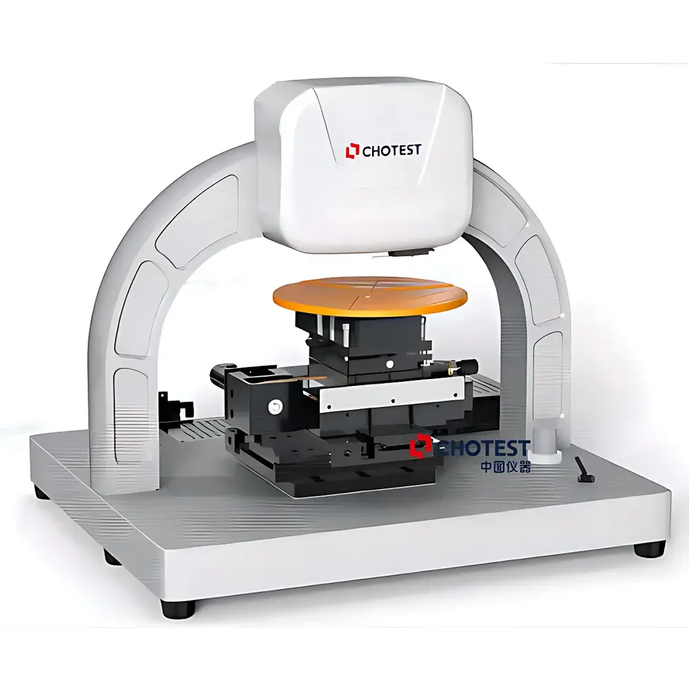
The Chotest NS200 Stylus Profilometer is a high-precision, contact-mode surface metrology instrument engineered for quantitative characterization of thin-film step heights, layer thicknesses, surface roughness, waviness, and macro-scale shape deviations—including wafer bow, warp, and radius of curvature. It operates on the principle of mechanical scanning profilometry: a 2 µm-radius diamond stylus traverses the sample surface under precisely regulated micro-force (1–50 mg), while an LVDC (Linear Variable Differential Capacitor) displacement sensor captures vertical deflection with sub-ångström resolution. This transduction method ensures exceptional signal-to-noise ratio and long-term stability—critical for repeatable measurement of ITO, SiO₂, SiNₓ, photoresists, and other functional thin films deposited via sputtering, CVD, ALD, spin-coating, or etching. The NS200’s monolithic龙门 (single-arch gantry) architecture minimizes structural compliance and environmental coupling, enabling traceable measurements compliant with ISO 25178-2 (areal surface texture) and ASTM E1399 (step height calibration standards). Its design meets foundational requirements for GLP-compliant labs and supports audit-ready data integrity when configured with time-stamped, user-logged measurement sessions.
Key Features
- Sub-ångström vertical resolution enabled by low-inertia LVDC capacitive sensing and active thermal drift compensation
- Programmable micro-force actuation (1–50 mg) with closed-loop electromagnetic control—ensures non-damaging contact on soft polymers, fragile oxides, and hard nitride films alike
- Integrated 5 MP color navigation camera with real-time probe path overlay and coordinate-mapped image stitching for rapid region-of-interest targeting
- Motorized XYZR-θ stage system: 150 mm × 150 mm XY travel, 360° continuous rotation, and precision Z-lift—enabling full spatial alignment without manual repositioning
- Single-scan length up to 55 mm with ultra-straight linear motion (<0.1 µm straightness error over full stroke), preserving true topographic fidelity
- Built-in SPC engine supporting Cp/Cpk calculation, control charting (X̄-R, I-MR), histogram distribution analysis, and automated outlier flagging per measurement series
Sample Compatibility & Compliance
The NS200 imposes no intrinsic constraints on sample reflectivity, electrical conductivity, or material hardness—making it suitable for opaque, transparent, conductive, insulating, brittle, or viscoelastic surfaces. It routinely measures ITO layers on glass substrates, SiO₂ trenches in silicon wafers, polymer lift-off profiles in MEMS fabrication, and anti-reflective coatings on optical lenses. All measurement data are timestamped, user-attributed, and stored in encrypted binary archives with checksum validation—supporting traceability under FDA 21 CFR Part 11 when paired with optional electronic signature modules. Calibration protocols follow NIST-traceable reference standards (e.g., NIST SRM 2131 for step height, ISO 25178-700 for roughness artifacts), and uncertainty budgets are documented per ISO/IEC 17025 guidelines. The instrument satisfies environmental specifications aligned with SEMI S2/S8 for semiconductor cleanroom deployment.
Software & Data Management
Chotest’s proprietary ProfilSoft™ v5.2 software provides a modular, scriptable interface compliant with Windows 10/11 x64 and supports both manual operation and fully automated batch workflows. Core capabilities include: custom scan path definition via absolute coordinates or relative offsets; intelligent navigation mapping using hybrid optical + tactile registration; multi-region measurement scripting for unattended wafer-level inspection; and export of point-cloud data in ISO-standardized formats (STL, XYZ, CSV, OPF). Raw profile traces retain full 16-bit depth and are archived with metadata (probe ID, force setting, environment log, operator ID). Audit trails record all parameter changes, file exports, and report generations—including who modified what and when—fulfilling GMP/GLP documentation requirements. Optional API integration enables direct linkage to MES or LabVantage LIMS platforms.
Applications
- Semiconductor process control: quantifying etch depth uniformity, CMP removal rates, and film stack thickness variation across 200 mm wafers
- Photovoltaic R&D: characterizing textured TCO layers, passivation stack interfaces, and laser scribing groove geometry
- Optical coating QA: verifying thickness gradients on broadband AR filters and measuring edge roll-off on dichroic mirrors
- MEMS/NEMS fabrication: profiling release etch undercuts, cantilever sidewall angles, and stiction-related deformation
- Advanced packaging: assessing solder bump height distribution, underfill fillet geometry, and redistribution layer (RDL) planarity
- Academic research: correlating nanoscale surface morphology with charge transport properties in perovskite thin films
FAQ
What is the maximum measurable step height, and how is linearity verified?
The NS200 supports step height measurements from <0.1 nm to 1000 µm. Linearity is validated annually using NIST SRM 2131 step height standards across five certified levels (10 nm–10 µm), with deviation ≤ ±0.5% of reading.
Does the system support automated wafer handling?
The NS200 is compatible with third-party semi-automated wafer loaders (SEMI E47.1 compliant); full automation requires integration with robotic end-effectors and custom motion sequencing scripts.
Can roughness parameters be calculated per ISO 4287 and ISO 25178 simultaneously?
Yes—ProfilSoft™ computes both profile-based (ISO 4287: Ra, Rz, Rq) and areal (ISO 25178-2: Sa, Sq, Sz) parameters from the same dataset, with selectable filtering (Gaussian, Spline, Robust) and segmentation logic.
Is thermal drift compensated during long-duration scans?
Yes—the LVDC sensor incorporates real-time temperature feedback, and the granite baseplate features embedded thermal mass stabilization; drift remains <0.15 nm/min over 2-hour continuous operation at constant ambient.
How is probe wear monitored and calibrated?
A dedicated probe qualification routine images the tip geometry via SEM correlation and tracks effective radius change; automatic force recalibration is triggered after every 100 hours of cumulative scan time or upon tip replacement.


