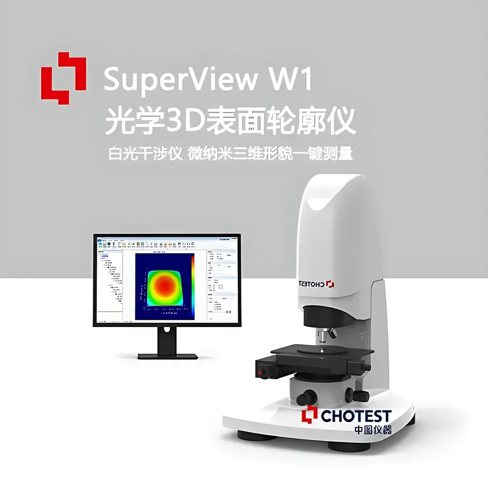
Chotest SuperViewW Advanced White Light Interferometric 3D Surface Profilometer
| Brand | Chotest |
|---|---|
| Origin | Guangdong, China |
| Model | W293 |
| Measurement Area | 140 × 100 mm |
| Type | Non-contact Optical 3D Surface Metrology System |
| Compliance | ISO 25178-2, ISO 25178-601, VDI/VDE 2634 Part 3 |
| Software Certification | FDA 21 CFR Part 11–compliant audit trail & electronic signature support (optional module) |
| Vertical Resolution | Sub-nanometer (≤0.1 nm typical) |
| Lateral Resolution | ≤0.5 µm (dependent on objective lens) |
| Z-Scan Range | Up to 10 mm (configurable with high-precision PZT or motorized stage) |
| Automation | Auto-focus, auto-fringe search, auto-brightness adjustment, multi-region stitching, programmable stage navigation |
Overview
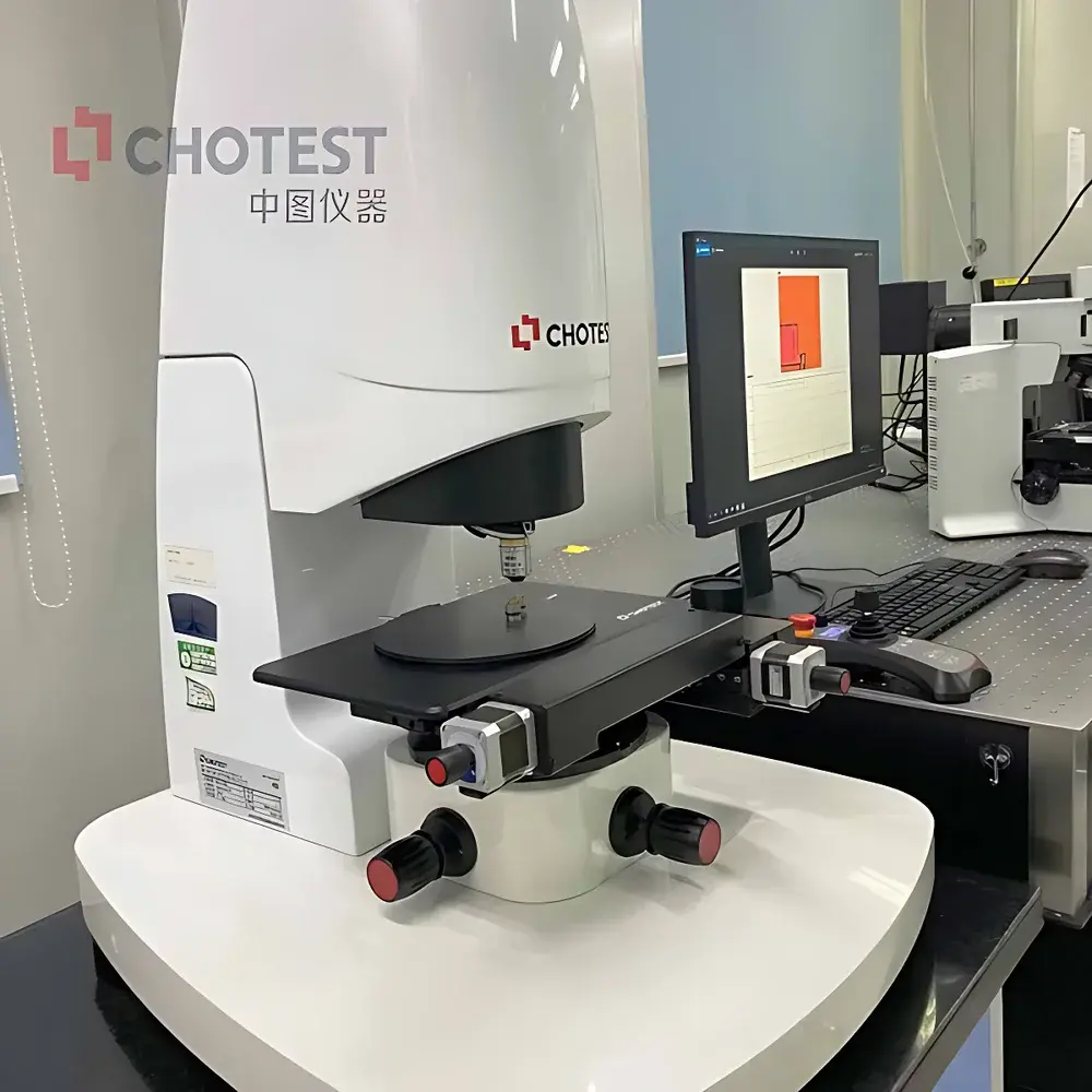
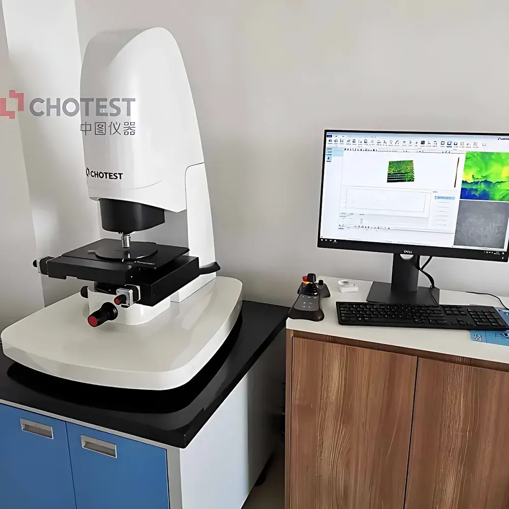
The Chotest SuperViewW is an advanced white light interferometric (WLI) 3D surface profilometer engineered for non-destructive, sub-nanometer topographic characterization of precision-engineered surfaces. Operating on the principle of low-coherence interferometry, it generates high-fidelity 3D surface maps by analyzing interference fringe contrast across a broadband visible spectrum. Unlike contact stylus profilers or confocal microscopes, the SuperViewW eliminates mechanical interaction—ensuring zero risk of surface damage, probe wear, or deformation artifacts—even on ultra-smooth substrates such as silicon wafers (Rq < 0.2 nm), fused silica optics, and thin-film-coated displays. Its optical architecture integrates a stabilized halogen or LED-based white light source, high-numerical-aperture objectives (5× to 100×), and a precision piezoelectric scanning stage, enabling simultaneous acquisition of height, slope, curvature, and texture parameters across macro-to-micro scale features.
Key Features
- Sub-nanometer vertical resolution (≤0.1 nm RMS repeatability) validated per ISO 25178-601 calibration protocols
- Large-field measurement capability: 140 × 100 mm scan area with seamless automated stitching—enabling full-wafer or panel-level metrology without manual repositioning
- Hybrid EPSI (Enhanced Phase-Shifting Interferometry) reconstruction algorithm: overcomes fundamental trade-offs between PSI’s limited vertical range and VSI’s reduced axial precision, delivering both high accuracy and extended Z-depth coverage
- Fully automated acquisition workflow: real-time auto-focus, intelligent fringe localization, adaptive illumination control, and stage-guided multi-site navigation
- Modular objective turret supporting magnifications from 2.5× to 100×, optimized for diverse surface classes—from super-polished optics (Ra < 0.3 nm) to structured MEMS textures (height > 50 µm)
- Rugged industrial-grade platform with vibration-damped granite base and environmental drift compensation algorithms
Sample Compatibility & Compliance
The SuperViewW accommodates rigid and semi-rigid planar or gently curved specimens up to 200 mm in diameter and 50 mm in height. It is routinely deployed in cleanroom environments (ISO Class 5–7) for semiconductor wafer inspection, glass substrate metrology in display manufacturing, and functional surface validation in medical device R&D. All measurement algorithms adhere to ISO 25178 series standards—including areal roughness (Sa, Sq, Sdr), hybrid parameters (Svk, Spk), and functional volume indices (Vmp, Vmc). Optional GLP/GMP-compliant software modules provide full 21 CFR Part 11 audit trails, user access controls, and electronic signature workflows—supporting regulated quality systems in pharmaceutical packaging, implantable device coating verification, and automotive sensor calibration.
Software & Data Management
The proprietary MetroPro™ analysis suite (v12.4+) delivers comprehensive post-processing capabilities via six modular toolsets: leveling & alignment, noise filtering (Gaussian, median, robust polynomial), region-of-interest extraction, form removal (least-squares, best-fit sphere/cylinder), spectral analysis (PSD, autocorrelation), and functional assessment (material ratio curves, bearing area, peak density). Batch processing supports concurrent analysis of hundreds of datasets with customizable report templates (PDF, CSV, XML). Raw interferogram data is stored in vendor-neutral HDF5 format, ensuring long-term archival integrity and third-party interoperability with MATLAB, Python (via h5py), and industry-standard metrology platforms.
Applications
- Semiconductor process control: quantifying CMP uniformity, etch depth variation, and defect morphology on 200/300 mm Si/SiC wafers
- Optical component certification: verifying surface irregularity (PV, RMS), scratch/dig compliance, and anti-reflective coating uniformity per MIL-PRF-13830B
- Consumer electronics: measuring touch sensor electrode height, cover glass curvature deviation, and laser-etched haptic feedback patterns
- Micro-opto-electro-mechanical systems (MOEMS): reconstructing actuator displacement profiles, mirror tilt angles, and comb-drive gap dimensions
- Advanced materials R&D: characterizing graphene transfer uniformity, battery electrode porosity distribution, and thermal barrier coating microcrack networks
FAQ
What is the minimum measurable surface roughness (Sa) achievable with the SuperViewW?
Typical Sa detection limit is 0.05 nm on calibrated reference flats under controlled environmental conditions (temperature stability ±0.5°C/h, acoustic isolation).
Can the system measure steep sidewalls or high-aspect-ratio structures?
Yes—when equipped with long-working-distance objectives and tilt-compensated stage control, it resolves slopes up to 75°; for steeper features, optional coherence scanning interferometry (CSI) mode extends lateral resolution without sacrificing Z-accuracy.
Is traceable calibration available for ISO/IEC 17025-accredited laboratories?
Chotest provides NIST-traceable step-height and roughness calibration artifacts (SRM 2101, 2102), along with on-site verification services compliant with ISO/IEC 17025 requirements.
How does the EPSI algorithm improve upon conventional PSI and VSI methods?
EPSI dynamically fuses phase-shifting and vertical-scanning data within each pixel, eliminating phase-unwrapping errors while maintaining nanometer-scale axial fidelity across multi-micron topographies—critical for measuring shallow trenches adjacent to tall pillars.
Does the software support custom parameter scripting or API integration?
Yes—the MetroPro SDK includes COM/ActiveX interfaces and Python bindings for automated measurement sequence orchestration, MES/SPC data push, and custom metric development.
Related Products


