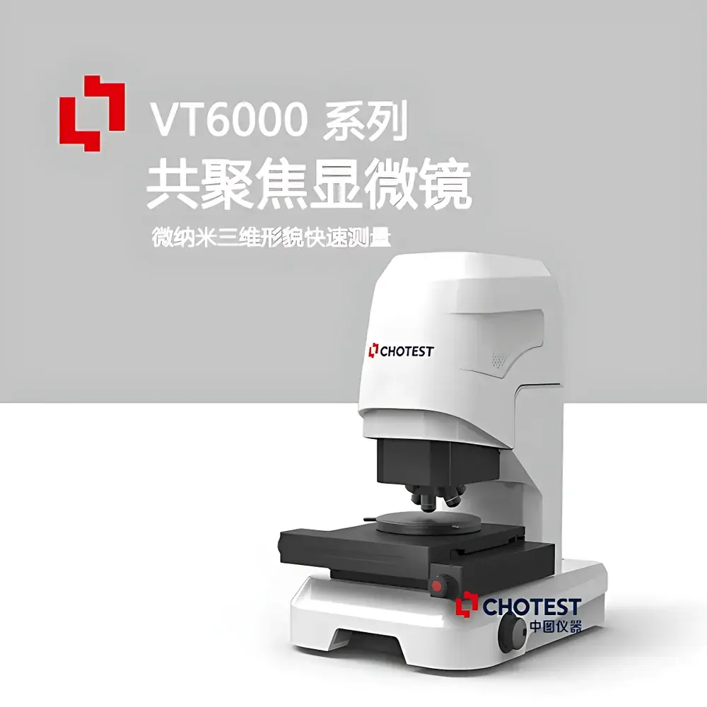
Chotest VT6000 Confocal 3D Surface Topography Microscope
| Brand | Chotest |
|---|---|
| Origin | Guangdong, China |
| Manufacturer Type | Authorized Distributor |
| Country of Origin | China |
| Model | VT6000 |
| Price | USD 132,000 (FOB Shenzhen) |
| Measurement Principle | Optical Confocal Imaging |
| Z-Scan Range | 10 mm |
| XY Travel | 100 mm × 100 mm |
| Z-Axis Resolution | ≤ 0.5 nm (typical, dependent on objective and signal-to-noise ratio) |
| Height Measurement Accuracy | ±0.8% of full scale |
| Objective Lenses | 10×, 20×, 50×, 100× (motorized 5-position turret) |
| Field of View | 1.2 mm × 1.2 mm (10×) to 120 µm × 120 µm (100×) |
| Light Source | Broadband White LED |
| Platform Load Capacity | 10 kg |
| Instrument Dimensions | 520 × 380 × 600 mm |
| Weight | 50 kg |
| Software | Integrated 3D metrology suite with automated batch analysis, GLP-compliant audit trail, and ISO 25178–compliant parameter calculation |
Overview
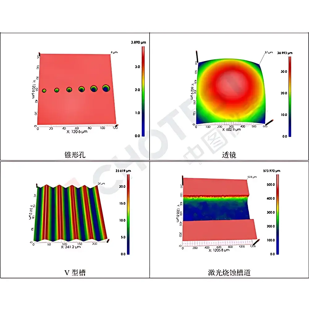
The Chotest VT6000 Confocal 3D Surface Topography Microscope is a non-contact optical metrology instrument engineered for high-resolution, quantitative surface characterization across industrial and research environments. It operates on the principle of point-scanning confocal microscopy—where a focused white-light beam is raster-scanned across the sample surface while a conjugate pinhole rejects out-of-focus light, enabling optical sectioning with nanoscale axial discrimination. Combined with precision motorized Z-axis scanning (up to 10 mm range) and high-stability XY translation stages, the VT6000 reconstructs true 3D topographic maps with sub-nanometer vertical resolution and micrometer-level lateral fidelity. Unlike conventional widefield or interferometric systems, the VT6000 maintains consistent measurement performance across surfaces with varying reflectivity (from <1% to >95%), roughness (Sa: 0.1 nm to 50 µm), and geometry—including steep sidewalls, deep trenches, and low-contrast microstructures such as solar cell pyramids or laser-scribed grooves. Its design adheres to core principles of traceable dimensional metrology, supporting compliance with ISO 25178 (Geometrical Product Specifications — Surface texture), ISO 4287/4288 (profile-based roughness), and ASTM E2923 (standard guide for 3D surface topography measurement).
Key Features
- Multi-mode acquisition: Supports single-field, multi-region, tile-based stitching, and fully automated batch measurement workflows—enabling seamless coverage of areas up to 100 mm × 100 mm without manual intervention.
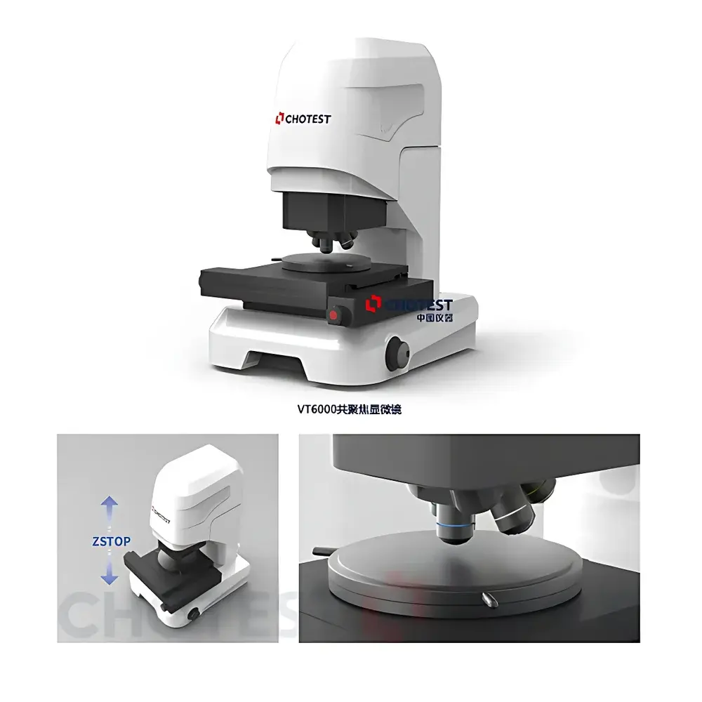
- Dual-stage Z-protection: Integrated mechanical + electronic end-stop sensors complement software-enforced ZSTOP logic, preventing objective–sample collision during coarse approach or script-driven scans.
- Motorized 5-position objective turret: Enables rapid switching between 10×, 20×, 50×, and 100× apochromatic objectives—each calibrated for parfocality and optimized for numerical aperture–dependent depth-of-field trade-offs.
- White-light LED illumination: Provides stable, cool, broadband spectral output (400–700 nm) with no laser safety constraints—ideal for routine lab use and long-duration stability-critical measurements.
- Real-time autofocus & drift compensation: Adaptive focus tracking algorithms maintain optimal focal plane during extended acquisitions, mitigating thermal or mechanical drift effects common in ambient-lab environments.
Sample Compatibility & Compliance
The VT6000 accommodates samples ranging from polished silicon wafers (Ra < 0.2 nm) to heavily textured photovoltaic surfaces (Rz > 20 µm), including transparent substrates (e.g., cover glass), coated metals, ceramics, polymers, and MEMS devices. No conductive coating or vacuum environment is required. All measurement data are timestamped and linked to instrument configuration logs, satisfying basic GLP documentation requirements. The system supports export of raw height maps in standard formats (e.g., .xyz, .stl, .tif) compatible with third-party analysis tools. While not FDA 21 CFR Part 11–certified out-of-the-box, the software architecture allows integration with enterprise-level validation frameworks for regulated QC environments (e.g., semiconductor fab process control or medical device R&D labs).
Software & Data Management
The proprietary MetroView™ analysis platform provides a unified interface for acquisition, visualization, and metrological reporting. Predefined measurement templates—configured per ISO 25178 parameters (Sa, Sq, Sz, Sdr, Vmp, Vvc, etc.) or custom user-defined metrics—ensure method consistency across operators and shifts. Batch processing enables concurrent analysis of hundreds of datasets with automatic report generation (PDF/Excel), including statistical summaries, pass/fail thresholds, and trend charts. All processing steps—including filtering (Gaussian, robust, spline), feature extraction (pores, peaks, valleys), and functional partitioning (bearing ratio, Abbott curve)—are fully logged with versioned metadata. Audit trails record operator ID, timestamp, parameter edits, and export actions—supporting internal quality audits and ISO 9001 compliance.
Applications
The VT6000 serves as a primary tool for surface form and finish verification in advanced manufacturing sectors. In semiconductor packaging, it quantifies laser scribe groove depth, width, and sidewall angle on dicing streets—directly correlating with die chipping yield. For photovoltaics, it measures aspect ratio and uniformity of screen-printed silver busbars and characterizes pyramid size/distribution in texturized Si wafers—parameters directly tied to anti-reflective performance and quantum efficiency. In optics manufacturing, it verifies surface flatness (PV, RMS) of precision lenses and molds; in automotive, it assesses wear scar geometry and coating delamination on engine components. Academic and national metrology labs utilize its traceable height calibration mode for inter-laboratory comparison studies and reference material certification.
FAQ
What surface roughness ranges can the VT6000 measure?
The system is validated for Sa values from sub-nanometer (e.g., epitaxial Si) to >50 µm (e.g., sandblasted metal), depending on objective selection and scan settings.
Does the VT6000 require vibration isolation?
A standard optical table is recommended for measurements below 1 nm vertical noise floor; for routine industrial QA (e.g., Ra > 10 nm), operation on a rigid benchtop is sufficient.
Can it measure transparent or semi-transparent layers?
Yes—the confocal principle enables interface detection at buried layer boundaries (e.g., thin-film coatings on glass), though quantitative thickness requires refractive index input and multi-surface modeling.
Is stitching accuracy traceable?
Tile alignment uses sub-pixel cross-correlation of overlapping regions; residual stitching error is typically < 0.1% of FOV and documented per ISO 10360-8 for coordinate measuring systems.
How is calibration maintained?
The system includes NIST-traceable step-height standards (100 nm–10 µm); daily verification using a certified grating sample is recommended per ISO/IEC 17025 guidelines.


