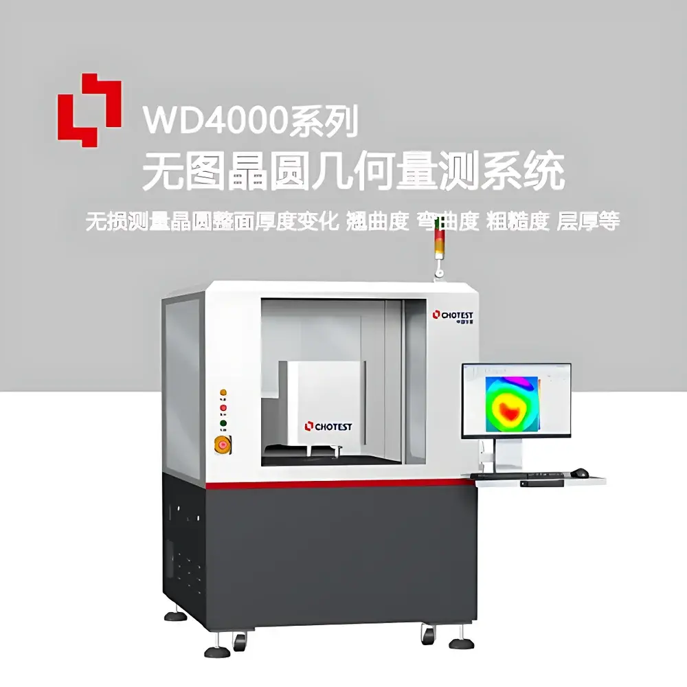
Chotest WD4000 Non-Contact Wafer Metrology System for Thickness, TTV, Bow, Warp, and 3D Topography
| Brand | Chotest |
|---|---|
| Origin | Guangdong, China |
| Manufacturer Type | Authorized Distributor |
| Country of Origin | China |
| Model | WD4000 |
| Price | USD 420,000 (FOB Shenzhen) |
| Thickness Range | 150 µm – 2000 µm |
| TTV/Bow/Warp Measurement Accuracy | ±0.1 µm (typical, calibrated per ISO 21287) |
| Z-Axis Resolution (Interferometry) | ≤ 0.1 nm |
| Lateral Scan Area | 400 mm × 400 mm |
| Vertical Travel | 75 mm |
| Maximum Wafer Size | 300 mm (12″) |
| Surface Reflectivity Range | 0.05% – 100% |
| Roughness RMS Repeatability | ≤ 0.005 nm (ISO 25178-6 compliant) |
| Interferometric Objective Options | 2.5×, 5×, 10×, 20×, 50× |
| Spectral Confocal Thickness Sensor | Dual-beam, high-stability SLED source, 90 µm measurement range (n = 1.5), minimum detectable thickness: 0.4 µm |
| Infrared Interferometry Module | SLED source, 37–1850 µm range |
| Scan Modes | Full-map, cross (‘X’), star (‘+’), user-defined multi-point |
| Compliance | ISO 5725 (accuracy & precision), ISO 25178-2 (areal texture), ISO 10110-7 (optical surface form), SEMI D39 (wafer geometry), ASTM F39 (silicon wafer bow/warp) |
Overview
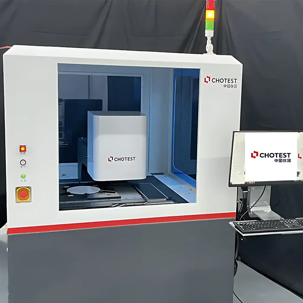
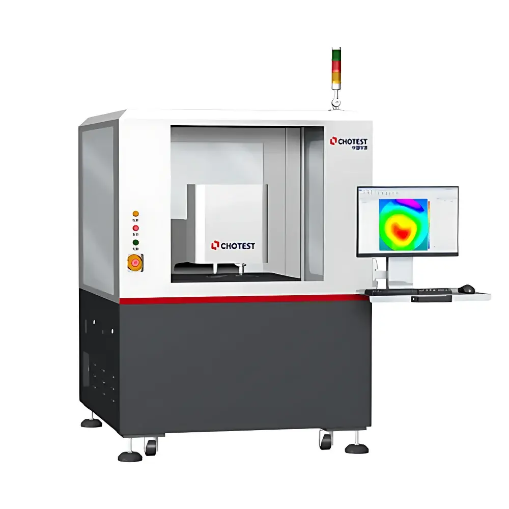
The Chotest WD4000 is a fully automated, non-contact metrology platform engineered for comprehensive geometric characterization of pattern-free semiconductor wafers. It integrates three synchronized optical sensing modalities—spectral confocal thickness mapping, white-light interferometry (WLI) for nanoscale 3D topography, and infrared interferometry for thick-film and substrate-level analysis—within a single, rigid granite-based龙门 (gantry) architecture. Unlike traditional stylus profilometers or segmented laser triangulation systems, the WD4000 employs a dual-path confocal alignment strategy for absolute thickness determination and a phase-shifting WLI engine with sub-nanometer Z-axis resolution to reconstruct full-field surface morphology without mechanical contact. This enables traceable, high-reproducibility measurement of critical wafer parameters—including total thickness variation (TTV), local thickness variation (LTV), bow, warp, site orientation repeatability index (SORI), total indicator reading (TIR), and surface roughness (Sa, Sq, Sz per ISO 25178)—across 150 mm to 300 mm substrates. The system is designed for integration into front-end process control environments where preservation of pristine surfaces, avoidance of particle generation, and compliance with cleanroom Class 100/ISO 5 protocols are mandatory.
Key Features
- Triple-sensor fusion architecture: Simultaneous spectral confocal (thickness), white-light interferometric (3D topography), and infrared interferometric (bulk film/subsurface) measurement channels.
- High-stability gantry platform: 400 mm × 400 mm × 75 mm travel envelope with AC servo direct-drive linear motors, granite base, and 0.1 µm-resolution optical encoders ensuring sub-micron positioning fidelity.
- Electrostatic-dissipative vacuum chuck: Perforated ceramic-coated chuck compatible with 100–300 mm wafers; maintains flatness under vacuum while preventing electrostatic discharge damage to sensitive epitaxial layers.
- Automated multi-objective turret: Motorized switching between 2.5×, 5×, 10×, 20×, and 50× interferometric objectives—enabling seamless transition from macro-form to nano-roughness analysis without manual intervention.
- Dual-stage vibration isolation: Passive air-spring base combined with active acoustic damping enclosure suppresses floor-borne and airborne noise, achieving < 0.5 nm RMS Z-noise in standard lab environments (per ISO 20486).
- Intelligent mark recognition & virtual fixturing: Machine vision algorithm detects wafer edge notches and flat/notch features to auto-align coordinate frame, eliminating manual centering and enabling repeatable multi-site mapping across production lots.
Sample Compatibility & Compliance
The WD4000 supports quantitative metrology on bare and coated wafers fabricated from silicon, silicon carbide (SiC), gallium arsenide (GaAs), gallium nitride (GaN), indium phosphide (InP), germanium (Ge), lithium niobate (LiNbO₃), sapphire, fused silica, and other optically transmissive or reflective semiconductor-grade substrates. Its wide dynamic reflectivity range (0.05%–100%) accommodates both highly polished mirror surfaces and matte-textured backgrind layers. All measurement algorithms adhere to international standards including ISO 25178-2 (areal surface texture), ISO 10110-7 (optical surface form tolerances), ISO 21287 (geometric product specification for wafer curvature), and SEMI D39 (standard test method for wafer bow and warp). Data audit trails, user access controls, and electronic signature support align with FDA 21 CFR Part 11 requirements for regulated manufacturing environments.
Software & Data Management
The proprietary Chotest MetroStudio™ software provides an integrated GUI for instrument control, real-time visualization, and statistical process analysis. It includes five core analytical modules: geometric contour analysis (step height, angle, curvature, straightness, roundness per ISO 1101), areal roughness analysis (full ISO 25178-2 parameter set), structural analysis (void volume, valley depth), frequency domain analysis (PSD, autocorrelation), and functional analysis (bearing ratio, material ratio curves). Raw interferograms and confocal intensity profiles are stored in HDF5 format with embedded metadata (timestamp, operator ID, calibration certificate ID, environmental conditions). Batch reporting complies with SPICE-compatible XML schemas and exports to JMP, Minitab, and factory MES via OPC UA or RESTful API. Audit logs record all parameter changes, measurement executions, and report generations with immutable timestamps—fully supporting GLP/GMP validation protocols.
Applications
The WD4000 serves as a reference-grade metrology tool across multiple semiconductor fabrication stages: pre-epitaxy substrate qualification (bow/warp screening per JEDEC JESD22-A115); post-grinding and polishing process monitoring (TTV and Sa stability tracking across 25+ repeated measurements); thin-film stack verification on compound semiconductor wafers (e.g., GaN-on-SiC layer thickness uniformity); and advanced packaging substrate inspection (copper pillar height, redistribution layer planarity). Its non-contact methodology eliminates risk of scratching delicate low-k dielectrics or fragile MEMS structures. In R&D labs, it enables correlation studies between thermal budget, CMP pressure, and resulting surface form deviation—feeding DOE models used in process window optimization.
FAQ
Does the WD4000 require physical contact with the wafer during measurement?
No. All measurement modes—spectral confocal thickness mapping, white-light interferometry, and infrared interferometry—are strictly non-contact and do not impose mechanical load on the sample.
Can the system measure wafers with anti-reflective coatings or low-reflectivity surfaces?
Yes. The optical design accommodates reflectivity as low as 0.05%, and adaptive gain control ensures stable signal acquisition across heterogeneous surface finishes.
Is the WD4000 validated for use in ISO Class 5 cleanrooms?
Yes. The system meets SEMI S2-0215 safety guidelines and operates within particle generation limits defined in ISO 14644-1 Class 5 when installed with optional HEPA-filtered purge air.
How is calibration traceability maintained?
Each system ships with NIST-traceable calibration artifacts (step-height standards, roughness samples, curvature references) and annual recalibration services aligned to ISO/IEC 17025-accredited laboratories.
What file formats are supported for data export and integration with factory systems?
MetroStudio™ supports CSV, XML (SPICE-compliant), HDF5, and PDF reports. Native OPC UA server and REST API enable bidirectional communication with MES, SPC, and CIM platforms.


