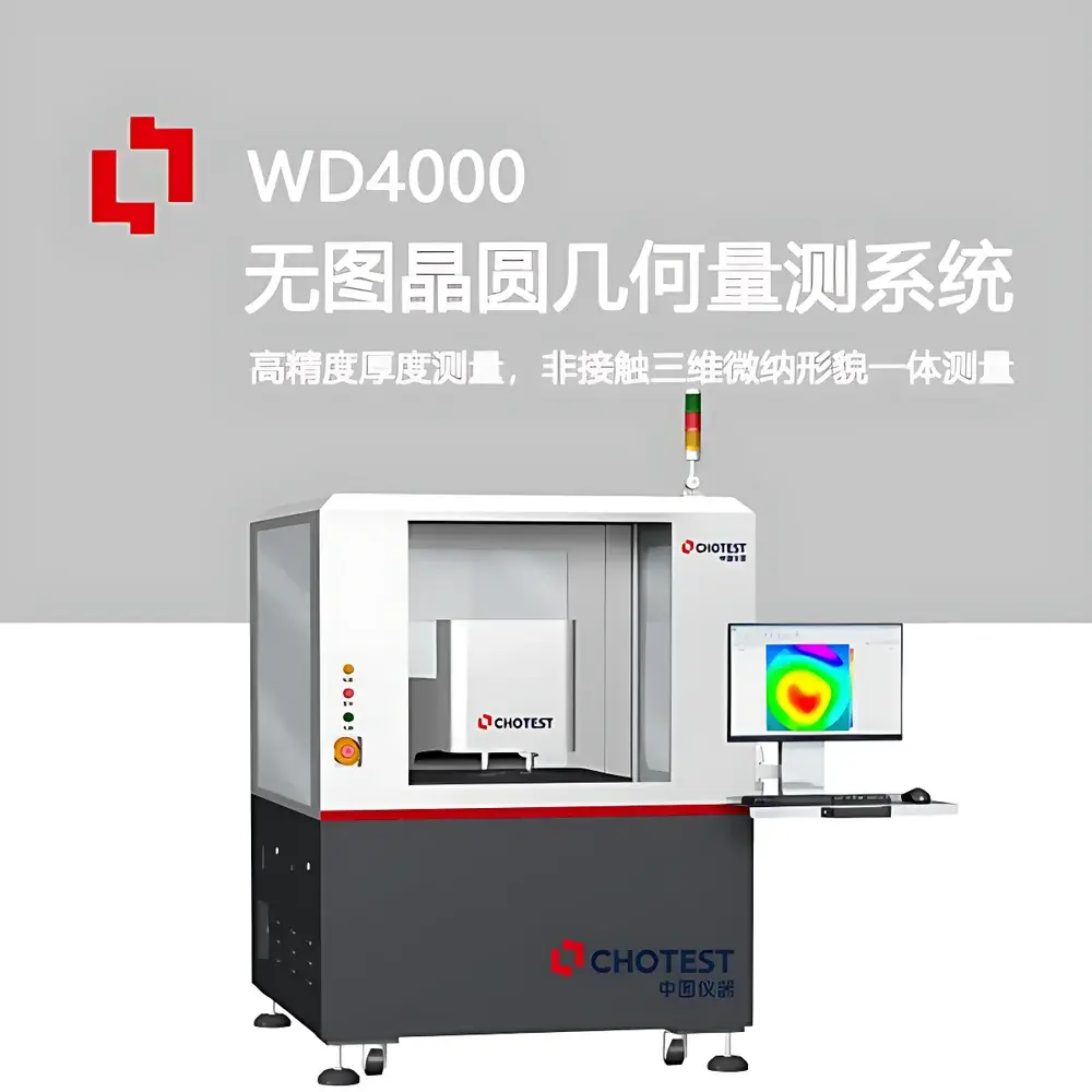
Chotest WD4000 Semiconductor Wafer Thickness and Warpage Metrology System
| Brand | Chotest |
|---|---|
| Origin | Guangdong, China |
| Model | WD4000 |
| Measurement Principles | Spectral Confocal Reflectometry (thickness), White-Light Interferometry (3D topography) |
| Wafer Compatibility | 4″–12″ |
| Max. Scan Area | 400 mm × 400 mm |
| Z-Axis Resolution | ≤ 0.1 nm |
| Thickness Range | 150 µm – 2000 µm |
| Surface Reflectivity Range | 0.05% – 100% |
| Roughness RMS Repeatability | ±0.005 nm |
| Motion Stage | Granite-based龙门 with AC servo direct-drive & 0.1 µm encoder resolution |
| Environmental Isolation | Active vibration damping for sub-nm stability |
Overview
The Chotest WD4000 Semiconductor Wafer Thickness and Warpage Metrology System is a fully integrated, non-contact metrology platform engineered for high-precision characterization of silicon and compound semiconductor wafers across front-end and back-end process flows. It combines dual physical measurement principles—spectral confocal reflectometry for nanoscale thickness profiling and white-light interferometry (WLI) for sub-nanometer vertical resolution 3D surface topography—to deliver comprehensive wafer-level geometric and morphological data in a single instrument. Designed to meet the stringent requirements of advanced node fabrication (≤28 nm), 3D IC stacking, and wide-bandgap device manufacturing (SiC, GaN, InP), the WD4000 performs full-map, cross-line, and user-defined multi-point scanning without mechanical contact, eliminating risk of surface scratching, particle generation, or electrostatic damage. Its architecture supports automated alignment via machine vision-based mark detection, programmable mapping routines, and real-time correction for thermal drift and stage nonlinearity—ensuring traceable, repeatable, and audit-ready measurements aligned with ISO/IEC 17025 and SEMI MF1530 guidelines.
Key Features
- Unified metrology engine delivering thickness, TTV, LTV, Bow, Warp, TIR, SORI, flatness, and 3D topography in one acquisition cycle
- Spectral confocal dual-beam sensing with <0.1 µm lateral resolution and ±0.3 µm absolute thickness accuracy across 150–2000 µm range
- White-light interferometric imaging with 0.1 nm Z-axis resolution, supported by precision piezo-scanning and adaptive fringe analysis algorithms
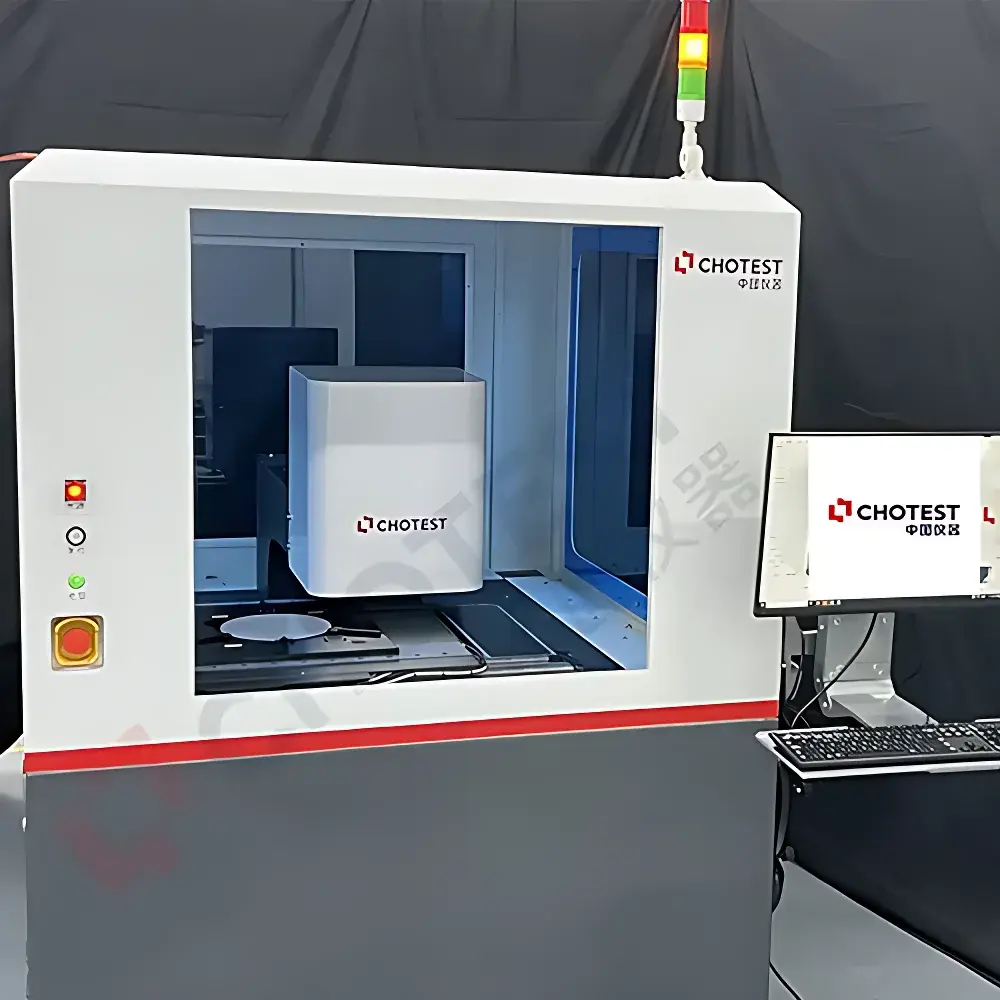
- Electrostatic-dissipative vacuum chuck with perforated design, compatible with 4″, 6″, 8″, and 12″ wafers—including fragile substrates such as GaAs, LiNbO₃, sapphire, and ultra-thin Si
- High-stability granite龙门 structure (400 × 400 × 75 mm travel), AC servo direct-drive axes, and 0.1 µm optical encoder feedback for sub-micron positioning fidelity
- Dual-stage vibration isolation system minimizing ambient acoustic and floor-borne noise to sustain <0.005 nm RMS repeatability in roughness measurement
- Motorized objective turret supporting interchangeable WLI objectives (2.5X, 5X, 10X, 20X, 50X) with auto-focus and parfocal calibration
- Integrated collision prevention: dual-sensor proximity monitoring + software-defined Z-limit safeguarding both objective lens and wafer surface
Sample Compatibility & Compliance
The WD4000 accommodates a broad spectrum of semiconductor and optoelectronic substrates—including Si, SiC, GaN, GaAs, InP, Ge, LiNbO₃, sapphire, fused silica, and glass—with surface reflectivity ranging from 0.05% (low-reflective epitaxial layers) to 100% (polished metal films). Its optical design enables stable fringe contrast on highly transparent, semi-transparent, and multilayer thin-film structures. All measurement protocols are configurable to comply with industry-standard test methods: ASTM F398 (wafer bow/warp), SEMI MF1530 (thickness uniformity), ISO 10722 (surface texture), and ISO 25178-2 (areal surface texture parameters). Data integrity is maintained through built-in GLP/GMP-compliant audit trails, user access control, and optional FDA 21 CFR Part 11 electronic signature support.
Software & Data Management
The proprietary Chotest MetroSuite™ software provides a unified interface for instrument control, data acquisition, and metrological analysis. It includes four core processing modules: Position Adjustment (image leveling, mirroring, coordinate transformation), Correction (spatial filtering, spike removal, scan line interpolation), Filtering (Gaussian, robust Gaussian, spline, spectral bandpass), and Extraction (region-of-interest selection, profile extraction, layer segmentation). Five analytical engines are embedded: Geometric Profile Analysis (step height, angle, curvature, straightness, circularity per ISO 1101), Roughness Analysis (full ISO 4287, ISO 25178, ISO 12781 compliance), Structural Analysis (volume, void depth, pit count), Frequency Analysis (PSD, autocorrelation, bandwidth filtering), and Functional Analysis (bearing ratio, material ratio curve, hybrid functional parameters). Raw data is stored in HDF5 format with metadata tagging for traceability; export options include CSV, STEP AP214, and metrology-specific XML schemas compliant with Fab-wide MES integration.
Applications
The WD4000 serves critical metrology roles across multiple domains: substrate quality screening (pre-epitaxy flatness verification), CMP process monitoring (post-CMP TTV and local thickness variation), SOI and bonded wafer inspection (bond interface uniformity), MEMS cavity depth profiling, display glass substrate warpage control (for OLED/LCD panel lamination), and advanced packaging (fan-out wafer-level packaging thickness mapping). It is widely deployed in R&D labs, foundry process development groups, and high-volume manufacturing environments where correlation between structural geometry and electrical performance must be quantified at wafer scale—particularly for power devices, RF filters, photonics, and heterogeneous integration platforms.
FAQ
What wafer sizes does the WD4000 support?
The system accommodates 4-inch, 6-inch, 8-inch, and 12-inch wafers using a programmable electrostatic vacuum chuck with customizable mounting patterns.
Does the WD4000 comply with semiconductor industry standards?
Yes—it supports measurement reporting per SEMI MF1530 (thickness), ASTM F398 (bow/warp), and ISO 25178-2 (3D surface texture), with optional validation documentation available upon request.
Can it measure low-reflectivity or transparent materials?
Yes—the spectral confocal sensor operates effectively on surfaces with reflectivity as low as 0.05%, and the WLI module includes coherence optimization for transparent and semi-transparent layers.
Is the system suitable for cleanroom deployment?
The WD4000 is Class 1000-compatible (ISO 6), features ESD-safe construction throughout, and offers optional HEPA-filtered air purge for extended operation in controlled environments.
How is measurement traceability ensured?
All optical and motion subsystems undergo factory calibration against NIST-traceable artifacts; certificate of calibration and uncertainty budget are provided with each unit.


