ECOPIA HMS-3000 / HMS-5000 Hall Effect Measurement System
| Brand | ECOPIA |
|---|---|
| Origin | South Korea |
| Model | HMS-3000 / HMS-5000 |
| Current Source Range | 1 nA – 20 mA |
| Resistivity Range | 10⁻⁵ – 10⁷ Ω·cm |
| Carrier Concentration Range | 1×10⁷ – 1×10²¹ cm⁻³ |
| Mobility Range | 1 – 1×10⁷ cm²/V·s |
| Magnetic Field Options | 0.37 T, 0.55 T, 1 T fixed |
| Sample Temperature | Ambient or 77 K (liquid nitrogen) |
| Sample Size Compatibility | 5×5 mm to 20×20 mm (optional 30 mm or 2-inch wafers) |
| Software Platform | Windows XP–10 compatible |
| Compliance | CE certified (July 2004) |
Overview
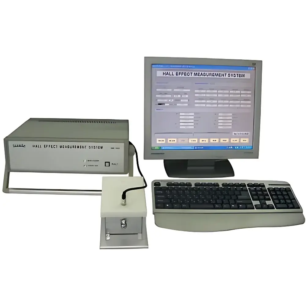
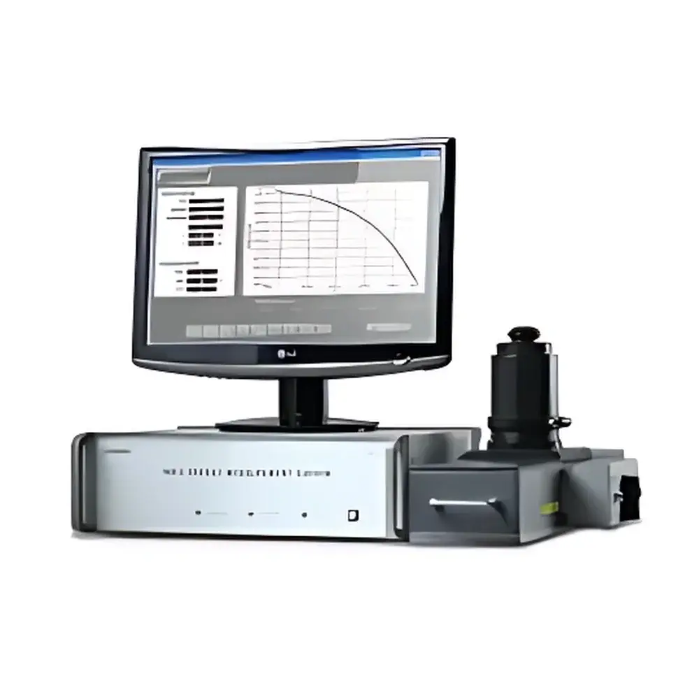
The ECOPIA HMS-3000 and HMS-5000 Hall Effect Measurement Systems are precision-engineered instruments designed for quantitative characterization of semiconductor thin films and bulk materials. Based on the classical Hall effect principle—where a transverse voltage develops across a current-carrying conductor under perpendicular magnetic field—the systems determine fundamental electronic transport parameters including bulk and sheet carrier concentration, carrier mobility, Hall coefficient, resistivity, sheet resistance, magnetoresistance, and vertical/horizontal resistance ratio. These measurements rely on the van der Pauw method, which eliminates geometric dependence by using four-terminal, non-contact probing configurations. The HMS platforms integrate a high-stability constant-current source, a van der Pauw terminal converter, cryogenic (77 K) sample stage, and calibrated permanent or variable magnetic field modules—enabling reproducible, standards-aligned measurements across research, process development, and quality assurance environments.
Key Features
- High-precision constant-current source with six programmable ranges (1 nA to 20 mA), minimizing measurement uncertainty through optimized current resolution and thermal drift compensation.
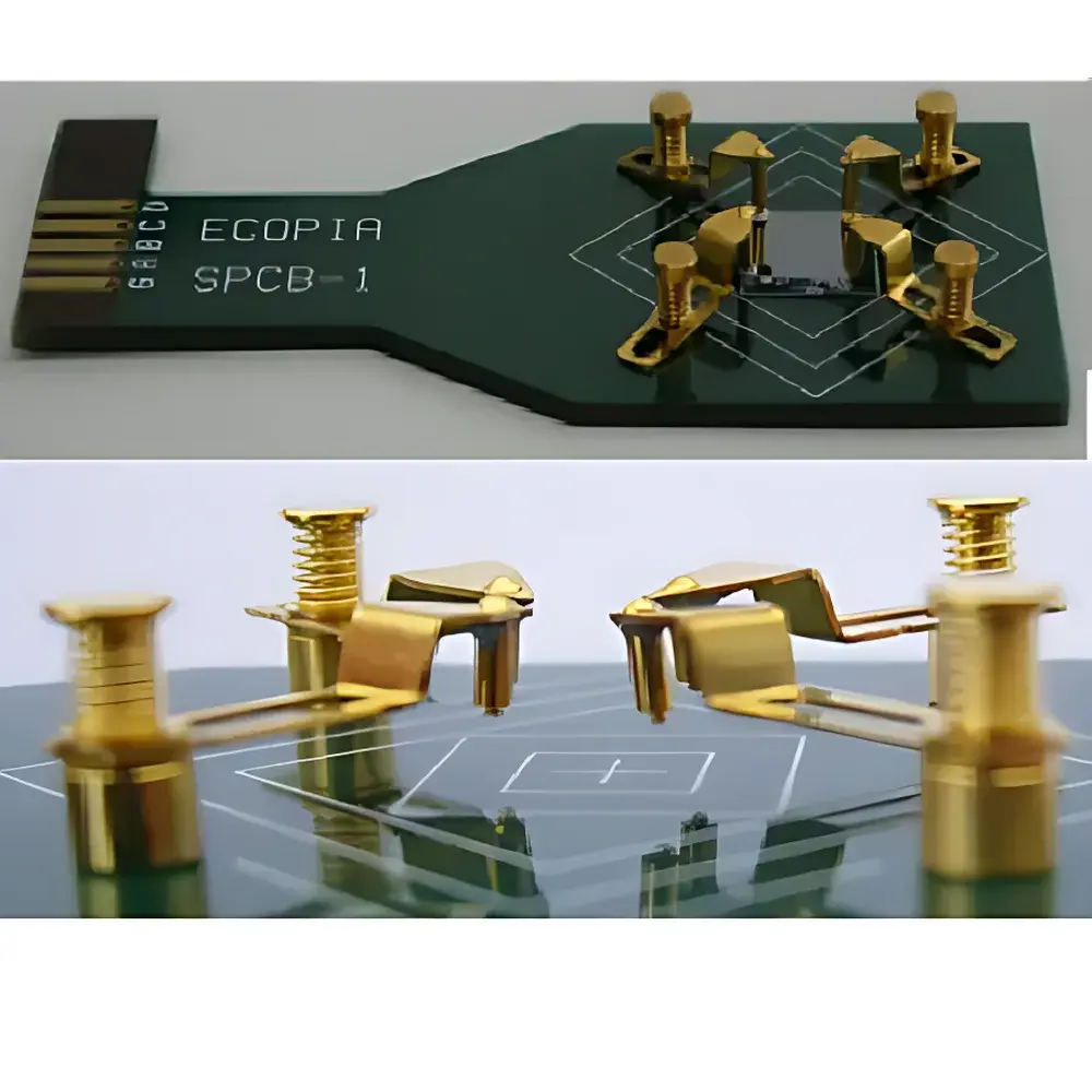
- Non-contact van der Pauw terminal switching architecture reduces parasitic noise and contact resistance artifacts, improving signal integrity especially for low-conductivity or fragile samples.
- Dual-temperature operation: ambient conditions for rapid screening and liquid nitrogen-cooled (77 K) configuration for low-temperature transport studies—compatible with standard Dewar assemblies.
- Modular sample holder design supports multiple substrate formats: rigid PCB boards (20×20 mm and 6×6 mm), spring-loaded SPCB fixtures for low-damage electrode contact, and dedicated wafer-compatible holders for up to 2-inch substrates.
- Integrated I–V and I–R curve acquisition enables real-time assessment of ohmic contact quality, linearity, and contact resistance—critical for validating device fabrication steps prior to Hall analysis.
- Patented hardware and algorithm architecture ensures data reproducibility via automated multi-cycle averaging, eliminating operator-dependent variability in repeated measurements.
Sample Compatibility & Compliance
The HMS systems support a broad spectrum of semiconductor materials—including Si, SiGe, SiC, GaAs, InP, InGaAs, GaN, ZnO, and transparent conductive oxides (e.g., ITO)—in both p-type and n-type configurations. Measurements conform to widely accepted metrology frameworks: van der Pauw methodology aligns with ASTM F76–22 (Standard Test Method for Measuring Resistivity of Semiconductor Materials) and ISO/IEC 17025 traceability requirements when used with calibrated reference standards. CE marking (certified July 2004) confirms compliance with EU electromagnetic compatibility (EMC Directive 2014/30/EU) and low-voltage safety (LVD Directive 2014/35/EU) directives. While not pre-certified for FDA 21 CFR Part 11, the software architecture supports audit-trail logging, user access control, and data export in CSV/Excel formats—facilitating integration into GLP/GMP-compliant laboratories upon local validation.
Software & Data Management
ECOPIA’s proprietary Windows-based software (compatible with XP through Windows 10) provides full instrument control, real-time visualization, and automated parameter derivation. The interface includes dual-mode operation: single-point measurement mode for routine QA/QC and sweep-mode for magnetic field– or temperature–dependent studies. All raw voltage/current data are logged with timestamps and metadata (field strength, temperature, current range, probe configuration). Calculated outputs include bulk carrier concentration (cm⁻³), sheet carrier density (cm⁻²), Hall mobility (cm²/V·s), Hall coefficient (cm³/C), resistivity (Ω·cm), sheet resistance (Ω/□), magnetoresistance (%), and anisotropic resistance ratios. Export functions support batch processing and third-party analysis in MATLAB, Python (NumPy/Pandas), or OriginLab. Software updates are distributed via secure download portal with version-controlled release notes.
Applications
- R&D labs characterizing novel channel materials (e.g., 2D semiconductors, perovskites, oxide heterostructures) for next-generation transistors and photodetectors.
- Fabrication facilities monitoring dopant activation, annealing efficacy, and interfacial charge trapping in epitaxial layers and heterojunctions.
- Quality control of sputtered or ALD-deposited TCO films (ITO, AZO) for display and PV applications—correlating sheet resistance with carrier density and mobility.
- Academic teaching laboratories demonstrating solid-state transport theory, Hall scattering mechanisms, and quantum corrections at low temperatures.
- Materials certification workflows requiring traceable resistivity and mobility data for ISO 9001 or IATF 16949-compliant documentation.
FAQ
What is the difference between HMS-3000 and HMS-5000 models?
The HMS-5000 extends the HMS-3000 platform with enhanced magnetic field flexibility (0.25–1 T variable electromagnet option), expanded low-current resolution (down to 100 pA), and optional integrated temperature controller for programmable cooling/heating stages beyond 77 K.
Can the system measure insulating or highly resistive materials?
Yes—the 10⁻⁵ to 10⁷ Ω·cm resistivity range accommodates semi-insulating GaAs and wide-bandgap oxides; however, optimal signal-to-noise requires proper guarding, shielding, and low-noise cabling for >10⁶ Ω·cm samples.
Is calibration required before each measurement?
No routine recalibration is needed; the system uses factory-trimmed current sources and Hall sensor calibration files stored in firmware. Users may perform verification checks using NIST-traceable resistivity standards (e.g., SRM 2135a).
How does the van der Pauw method handle irregularly shaped samples?
It inherently eliminates geometric dependency—only requiring four ohmic contacts placed anywhere on the sample perimeter, making it ideal for patterned wafers, irregular flakes, or non-rectangular thin-film deposits.
Does the software support automated reporting for regulatory submissions?
While not out-of-the-box 21 CFR Part 11 compliant, the software generates timestamped, user-attributed reports with digital signatures and immutable log files—enabling internal validation for regulated environments.


