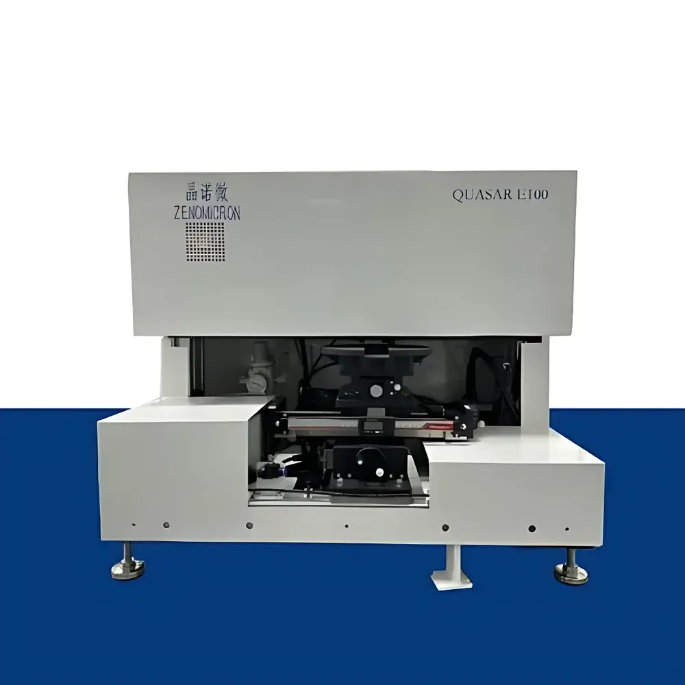
Ellipsometer E100 by ZENO
| Brand | ZENO |
|---|---|
| Model | E100 |
| Type | Spectroscopic Ellipsometer |
| Form Factor | Benchtop |
| Measurement Principle | Null- and Rotating-Analyzer-Based Spectroscopic Ellipsometry (SE) |
| Wavelength Range | 240–1700 nm (configurable UV-VIS-NIR) |
| Spot Size | Standard 3 mm Ø |
| Substrate Compatibility | 4″ to 12″ wafers, irregular shapes, rigid/flexible substrates |
| Measured Parameters | Film thickness (sub-nm resolution), complex refractive index (n + ik), extinction coefficient (k), interfacial roughness, optical bandgap |
| Precision | ≤0.01 nm RMS repeatability on SiO₂/Si reference samples (t < 30 nm, n=30 measurements) |
| Compliance | ASTM F1599, ISO 15632, SEMI MF1530 |
| Software | ZENO-EllipSuite v4.x with GLP-compliant audit trail, user role management, and 21 CFR Part 11-ready data export |
| Automation Options | Motorized XYZ stage, auto-alignment module, wafer handler integration |
| Origin | Shanghai, China |
| Distribution | Authorized Global Distributor Network |
Overview
The ZENO Ellipsometer E100 is a high-performance benchtop spectroscopic ellipsometer engineered for precision metrology of thin-film optical constants and thickness in semiconductor process development, R&D laboratories, and advanced materials manufacturing. Operating on the fundamental principles of polarization-state modulation—specifically rotating-analyzer ellipsometry combined with broadband spectral acquisition—the E100 quantifies the change in polarization state (Δ and Ψ) of light reflected from a sample surface across a wide spectral range (240–1700 nm). This enables model-based extraction of critical optical parameters including film thickness (with sub-nanometer resolution), complex refractive index (n + ik), extinction coefficient (k), interfacial layer density, and effective medium composition. Unlike intensity-based reflectometers, ellipsometry is inherently insensitive to ambient light, beam intensity fluctuations, and detector nonlinearity—delivering superior accuracy and long-term stability for ultra-thin films (<1 nm) and multilayer stacks common in gate oxides, high-k dielectrics, ALD precursors, and transparent conductive oxides.
Key Features
- Broadband spectral acquisition (UV-VIS-NIR) with configurable grating and detector options to optimize signal-to-noise ratio for specific material systems
- Sub-1 nm thickness resolution on SiO₂/Si reference structures, validated per ASTM F1599 protocols
- Motorized precision alignment stage with real-time beam positioning feedback and auto-focus capability
- Modular optical head design supporting interchangeable light sources (Xe lamp, LED arrays, or tunable laser diodes) for application-specific wavelength optimization
- Micro-spot measurement mode (down to 50 µm diameter) for localized analysis of patterned wafers, defects, or heterogeneous coatings
- Robust mechanical architecture with vibration-damped granite base and temperature-stabilized optical path for high reproducibility in non-cleanroom environments
Sample Compatibility & Compliance
The E100 accommodates substrates ranging from 4-inch to 12-inch silicon wafers, as well as non-standard geometries—including glass slides, flexible polymer foils, metal coupons, and ceramic substrates—without requiring custom fixtures. Its open-stage design allows direct mounting of samples up to 300 mm × 300 mm. All measurement workflows comply with industry-standard traceability frameworks: data acquisition adheres to ISO 15632 for ellipsometric characterization, while software operation supports GLP/GMP-aligned documentation requirements. The system meets SEMI MF1530 specifications for thin-film metrology in semiconductor fabrication facilities and includes built-in calibration routines traceable to NIST-certified reference standards.
Software & Data Management
ZENO-EllipSuite v4.x provides a unified interface for instrument control, optical modeling (via Cauchy, Tauc-Lorentz, Cody-Lorentz, and B-spline dispersion models), regression analysis, and statistical reporting. Each measurement session generates timestamped, digitally signed records containing raw Ψ/Δ spectra, fitting residuals, parameter covariance matrices, and full model definitions. Audit trails log all user actions—including parameter edits, model changes, and report exports—with immutable timestamps and operator IDs. Export formats include CSV, XML, and HDF5, fully compatible with enterprise LIMS and MES platforms. Optional 21 CFR Part 11 compliance package enables electronic signatures, role-based access control, and secure archival for regulated environments.
Applications
- Process monitoring of atomic layer deposition (ALD) and chemical vapor deposition (CVD) layers in front-end-of-line (FEOL) integration
- Characterization of high-k/metal gate stacks, SiGe channel layers, and epitaxial growth uniformity
- Optical constant determination for perovskite absorbers, CIGS, and amorphous silicon in photovoltaic R&D
- Quality assurance of anti-reflective, ITO, and AZO coatings on display glass and touch sensors
- Interfacial oxidation kinetics studies during thermal annealing or plasma exposure
- Non-destructive evaluation of corrosion inhibition films and self-assembled monolayers (SAMs)
FAQ
What is the minimum measurable film thickness on silicon substrates?
The E100 achieves reliable quantification of SiO₂ films down to 0.3 nm on Si(100), with statistical repeatability ≤0.01 nm RMS for t < 30 nm under controlled lab conditions.
Can the system measure multi-layer stacks with buried interfaces?
Yes—using physically constrained optical models and iterative regression, the E100 resolves up to 7-layer stacks (e.g., Si/SiO₂/HfO₂/TiN) provided sufficient spectral contrast and appropriate starting parameters.
Is vacuum or nitrogen purging required for UV measurements below 250 nm?
For measurements extending below 240 nm, optional nitrogen purge or vacuum-compatible optical path configuration is available to minimize atmospheric O₂ absorption.
Does the software support automated recipe-based measurements for production line deployment?
Yes—ZENO-EllipSuite includes batch scripting, trigger-based acquisition, and pass/fail threshold logic for inline process control integration.
How is calibration maintained over time?
The system performs daily self-calibration using an integrated reference mirror and certified Si/SiO₂ standards; full recalibration is recommended annually or after major hardware service events.


