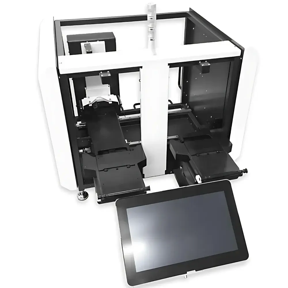
EMU SPPE Single-Wafer Pick-and-Place System
| Brand | EMU |
|---|---|
| Origin | UK |
| Manufacturer Type | Authorized Distributor |
| Import Status | Imported |
| Model | SPPE |
| Throughput | 400 WPH |
| Wafer Diameters Supported | 75 mm / 100 mm, 125 mm / 150 mm, and 150 mm / 200 mm |
| ESD Protection | Full Integrated ESD-Safe Architecture |
| Compatibility | Si, SiC, GaN, and Other Semiconductor Substrates |
| Control System | Embedded PC with Touchscreen HMI |
| Interface Options | SECS/GEM Compliant |
| Cassette Handling | Auto-mapping with Dual-Slot & Cross-Loading Detection |
| Safety | Real-time Wafer Presence & Edge Detection Sensors |
Overview
The EMU SPPE Single-Wafer Pick-and-Place System is a precision-engineered semiconductor handling platform designed for high-integrity transfer of bare wafers between standard FOUPs, FOSBs, or open cassettes in front-end and back-end cleanroom environments. Operating on a non-vacuum end-effector principle—utilizing electrostatic or mechanical clamping mechanisms—the SPPE eliminates vacuum-related particulate generation and wafer warpage risks common in traditional vacuum-based handlers. Its core architecture follows the proven Recif/EMU SPP lineage, with continuous evolution since initial deployment in wafer fabs worldwide beginning in the late 1990s. The system supports full-diameter flexibility across 75 mm to 200 mm substrates—including heterogeneous materials such as silicon (Si), silicon carbide (SiC), and gallium nitride (GaN)—and accommodates variable wafer thicknesses (e.g., 150–775 µm) without mechanical reconfiguration. All motion control, cassette mapping, and safety logic are executed via an integrated industrial PC running deterministic real-time firmware, ensuring sub-millisecond response for critical alignment and collision avoidance.
Key Features
- Non-vacuum wafer gripping technology minimizes particle shedding and surface contamination during transfer.
- Automated cassette mapping with real-time dual-slot detection and cross-loading verification prior to any handling operation.
- Full ESD-safe design compliant with ANSI/ESD S20.20 and IEC 61340-5-1 standards, including grounded stainless-steel frame, conductive belts, and static-dissipative end-effectors.
- Embedded PC-based controller with intuitive touchscreen HMI supporting multi-language UI configuration (English, Japanese, Korean, Chinese).
- Modular hardware architecture enabling rapid field upgrades for new wafer sizes—no structural retrofit required for transitions between 75/100 mm, 125/150 mm, or 150/200 mm configurations.
- SECS/GEM interface certified to SEMI E30 (GEM) and E4 (SECS-II) standards, enabling seamless integration into factory automation systems (FAS) and MES platforms.
- Dual-stage safety monitoring: optical edge sensors verify wafer presence and centering during loading/unloading; proximity switches confirm cassette position and lid status.
Sample Compatibility & Compliance
The SPPE handles unpatterned and patterned wafers across all major semiconductor substrate families: crystalline silicon (Czochralski and float-zone), silicon-on-insulator (SOI), compound semiconductors (SiC, GaN, GaAs), and emerging wide-bandgap materials. It accepts industry-standard carriers including 25-slot plastic cassettes (e.g., Entegris C-Series), SMIF pods, and FOUPs (SEMI E47.1 compliant). Wafer thickness range spans 150 µm to 775 µm, accommodating thin-wafer grinding and temporary bonding applications. Mechanical tolerances meet SEMI S2 (Safety Guidelines) and S8 (Mechanical Interfaces) specifications. Electrical safety complies with UL 61010-1 and EN 61010-1. ESD performance is validated per IEC 61340-2-3 (charge decay testing) and includes continuous ground-path monitoring with alarm logging.
Software & Data Management
The SPPE runs proprietary EMU MotionWare™ firmware, providing recipe-driven operation with version-controlled process definitions stored locally and exportable via USB or network share. Each recipe defines carrier type, wafer diameter, thickness compensation offset, acceleration profiles, and sensor sensitivity thresholds. Audit trails record all operator actions, error events, and maintenance interventions—supporting GLP/GMP traceability requirements. Optional data export modules generate CSV logs compatible with statistical process control (SPC) software (e.g., InfinityQS, Minitab). Firmware updates are delivered via signed package files with SHA-256 checksum verification. Remote diagnostics support is available through secure TLS-encrypted VNC sessions, subject to customer-defined firewall policies.
Applications
- Front-end wafer sort: pre- and post-probe station loading/unloading for electrical test.
- Back-end packaging: die attach prep, wafer-level packaging (WLP) substrate alignment, and temporary bonding/debonding workflows.
- Research & development labs: flexible handling of prototype wafers with non-standard geometries or fragile coatings.
- Failure analysis (FA) preparation: precise placement onto SEM stubs or cross-section fixtures without edge chipping.
- Quality assurance: automated sampling from production lots for metrology or defect review stations.
FAQ
Does the SPPE support both manual and automated mode operation?
Yes—the system operates in either fully automatic mode (integrated with factory host) or semi-automatic mode with operator-initiated steps via touchscreen, including manual override for cassette loading and emergency stop recovery.
Can the SPPE be retrofitted for future wafer size expansions?
Yes—hardware modularity allows field upgrade to larger diameters using certified kit components; no replacement of mainframe or controller is required.
Is the SECS/GEM interface pre-certified for specific fab host systems?
EMU provides conformance reports against SEMI E30 and E4 standards; site-specific integration validation is performed during commissioning with customer’s host equipment.
What maintenance intervals are recommended for long-term reliability?
Preventive maintenance is scheduled every 1,000 operating hours or annually—whichever occurs first—with documented procedures covering belt tension calibration, sensor alignment verification, and ESD path resistance testing.
How does the SPPE handle warped or cracked wafers?
Integrated optical edge detection identifies non-planar wafers exceeding ±25 µm total indicator reading (TIR); the system halts transfer and logs a classification-level fault code for operator review.


