English Product Name
| Brand | AML |
|---|---|
| Origin | United Kingdom |
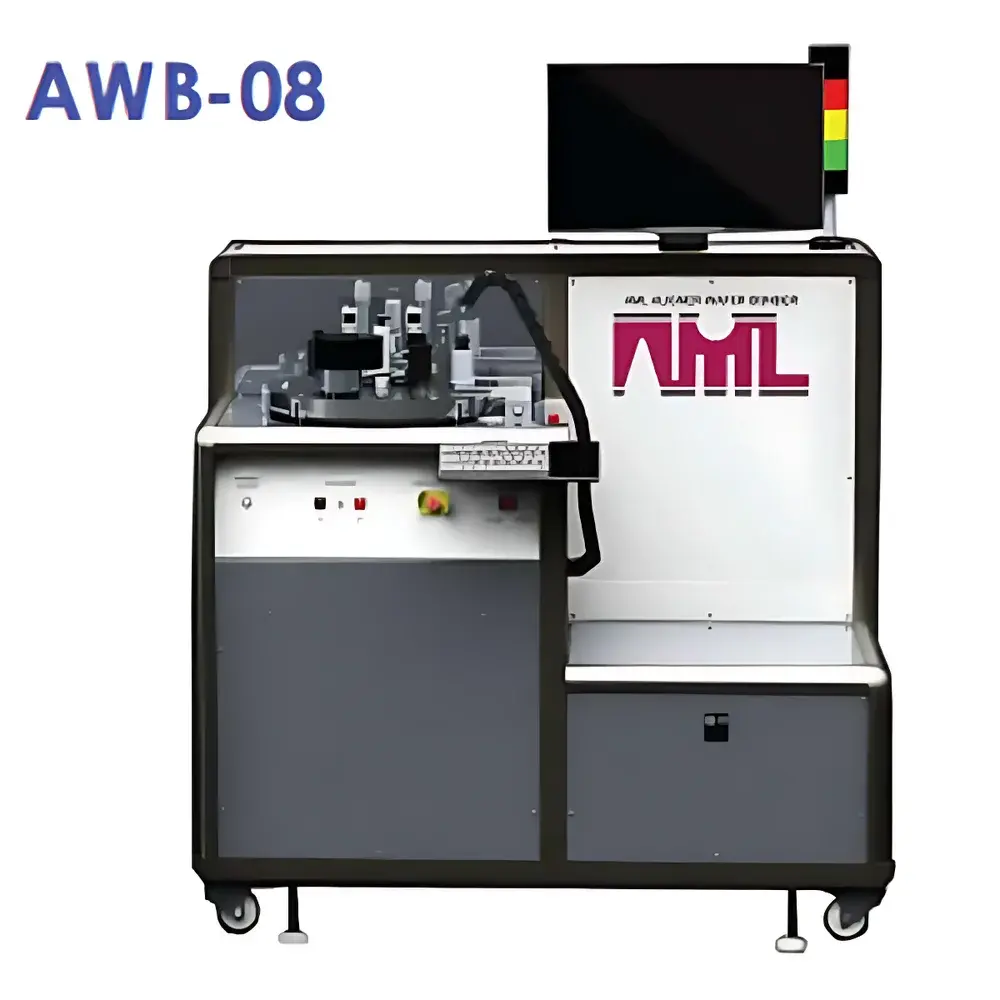
| Model | AWB-04, AWB-08, ROCK-04, ROCK-08 |
| Wafer Size Support | Up to 200 mm |
| Maximum Bonding Temperature | 650 °C |
| Heating Control | Independent top/bottom platen |
| Vacuum Level | ≤10⁻⁵ mbar (with turbomolecular pump) |
| Bonding Processes Supported | Anodic, Thermocompression, Eutectic, Glass Frit, Direct Si–Si, Intermediate Layer Adhesive, SOI, and Plasma-Activated Bonding |
| Automation Level | Semi-automatic (manual load/unload, fully automated bonding cycle) |
| Nanopatterning Capability | Integrated nanoimprint functionality |
Overview
The AML AWB and ROCK series are precision-engineered in-situ alignment wafer bonding systems designed for R&D and low-to-medium volume production environments in semiconductor, MEMS, and advanced packaging facilities. These systems implement real-time optical alignment—performed under vacuum or controlled atmosphere—immediately prior to bond initiation, eliminating post-alignment drift and ensuring sub-micron overlay accuracy across full 200 mm wafers. The bonding principle relies on controlled thermomechanical compression combined with electrostatic field application (for anodic bonding) or surface activation (e.g., plasma or thermal oxidation), enabling atomic-level interface formation between dissimilar or identical substrates. Each system integrates three core functions—alignment, surface activation (optional), and bonding—within a single vacuum chamber, minimizing contamination risk and process variability. Engineered for high reproducibility, the platform supports all major wafer bonding methodologies recognized in ISO/IEC 17025-compliant laboratories and aligns with key industry standards including SEMI S2/S8, ASTM F1791 (for MEMS packaging), and JEDEC JEP167 (for 3D IC reliability testing).
Key Features
- In-situ optical alignment with motorized X/Y/θ stages and high-resolution CCD imaging, enabling real-time overlay verification at <1 µm accuracy before bond initiation
- Independent top and bottom platen heating control (up to 650 °C) with ±0.5 °C uniformity across 200 mm wafers, verified per ASTM E220 calibration protocols
- High-vacuum bonding chamber (<10⁻⁵ mbar base pressure, achievable with integrated turbomolecular pumping station) for oxide-free interfaces and low-defect bonding
- Modular chamber architecture supporting interchangeable tooling for anodic, thermocompression, eutectic, glass frit, and direct silicon bonding—each with dedicated pressure/temperature/time parameter sets
- Integrated nanoimprint capability via optional heated stamp module, compatible with UV-curable and thermal resists for hybrid bonding + patterning workflows
- Semi-automated operation: manual wafer loading/unloading with fully programmable, recipe-driven bonding cycles—including ramp/soak profiles, multi-step pressure application, and real-time sensor logging
Sample Compatibility & Compliance
The AML AWB/ROCK platforms accommodate standard silicon, quartz, glass, sapphire, SiC, GaN, and LTCC substrates ranging from 50 mm to 200 mm diameter, including patterned, thinned, or bonded carrier wafers. Chuck design supports both flat and warped wafers (up to 50 µm bow) using adaptive vacuum distribution. All bonding processes comply with ISO 14644-1 Class 5 cleanroom integration requirements. System validation documentation supports GLP/GMP audit readiness, including IQ/OQ/PQ templates aligned with FDA 21 CFR Part 11 data integrity guidelines. Process recipes are traceable with electronic signature support, and temperature/pressure/vacuum logs are timestamped and exportable in CSV or XML format for regulatory submission.
Software & Data Management
Control is executed via a Windows-based HMI running AML’s proprietary BondMaster™ software suite. The interface provides intuitive recipe creation with nested process steps, conditional logic (e.g., “hold until vacuum <5×10⁻⁵ mbar”), and interlock monitoring (door status, cooling water flow, overtemperature cutoff). Real-time graphs display simultaneous trends for upper/lower platen temperature, chamber pressure, applied force, and alignment error vectors. All operational data—including operator ID, timestamp, recipe version, and sensor readings—is stored in an encrypted local SQL database with automatic daily backup. Audit trail functionality meets ALCOA+ principles (Attributable, Legible, Contemporaneous, Original, Accurate, Complete, Consistent, Enduring, Available), and raw data exports are compatible with JMP, MATLAB, and MES integration via OPC UA.
Applications
These systems serve as foundational tools in multiple high-value fabrication domains: MEMS inertial sensor and microfluidic device manufacturing (e.g., pressure sensors, lab-on-chip platforms); SOI substrate preparation for RF-SOI and FD-SOI CMOS; 3D heterogeneous integration (chiplet assembly, TSV-enabled interposers); compound semiconductor power devices (GaN-on-Si, SiC die bonding); and emerging applications such as quantum photonic chip packaging and micro-LED transfer bonding. Their ability to execute low-stress, high-yield bonds on fragile or thermally mismatched substrates makes them particularly suited for R&D prototyping where process flexibility and metrology-grade repeatability are prioritized over throughput.
FAQ
What wafer sizes does the AWB-08 support?
The AWB-08 is configured for 200 mm wafers and maintains full compatibility with smaller formats (150 mm, 100 mm, and 76 mm) using adjustable chucks and alignment fiducial libraries.
Is vacuum level monitored and logged during bonding?
Yes—capacitance manometers provide continuous chamber pressure measurement with 0.1 mbar resolution; all values are time-stamped and archived alongside thermal and mechanical parameters.
Can the system perform low-temperature bonding for polymer substrates?
Absolutely—the independent platen control enables asymmetric heating (e.g., 120 °C top / 25 °C bottom), supporting adhesive bonding of PI, PET, or PDMS layers without thermal degradation.
How is alignment accuracy verified pre-bond?
Through automated image correlation of alignment marks using sub-pixel interpolation algorithms, with uncertainty quantified per ISO 10110-5 and reported in the final process log.
Does AML provide process qualification support?
Yes—AML offers on-site process development services, including DOE-based optimization, bond strength validation (ASTM F1188 shear testing), and cross-sectional TEM sample preparation guidance.


