English Product Name
| Brand | Germanlitho (Tianren Micronano) |
|---|---|
| Origin | Shandong, China |
| Manufacturer Type | OEM Manufacturer |
| Origin Category | Domestic (China) |
| Model | GL8 CLIV Gen2 |
| Pricing | Upon Request |
Overview
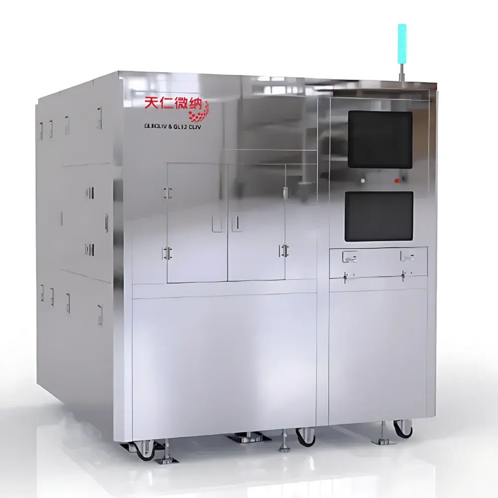
The Germanlitho GL8 CLIV Gen2 is a production-grade, full-field ultraviolet nanoimprint lithography (UV-NIL) system engineered for high-fidelity replication of nanoscale patterns on 200 mm substrates. It implements the proprietary Contact Lithography in Vacuum (CLIV) process—a vacuum-assisted, conformal contact technique that minimizes air entrapment and interfacial defects during mold-substrate engagement. This enables robust pattern transfer with sub-10 nm critical dimension (CD) accuracy and aspect ratios exceeding 10:1—critical for advanced diffractive optical elements (DOEs), AR/VR waveguide gratings (including slanted-profile gratings), high-density biochips, micro-LED arrays, and microlens arrays. Unlike conventional soft or thermal NIL platforms, the CLIV architecture ensures uniform mechanical contact across the entire 200 mm field, mitigating edge distortion and residual layer variation—key challenges in large-area nanofabrication. The system operates under controlled internal cleanroom conditions (Class 10 or better) and integrates electrostatic discharge (ESD) mitigation to preserve substrate integrity and mold longevity.
Key Features
- Full-field UV-NIL platform optimized for 200 mm wafers and flat substrates (2″, 100 mm, 150 mm, and custom sizes available)
- CLIV technology: vacuum-assisted conformal contact ensures defect-free imprinting of high-aspect-ratio nanostructures with <10 nm CD fidelity
- Integrated high-power UV-LED area source (365 nm, >1000 mW/cm² irradiance; optional 2000 mW/cm² and multi-wavelength configurations)
- Water-cooled illumination module for thermal stability and long-term LED lifetime
- Automated workflow: auto-alignment (optional optical edge detection), auto-imprinting, UV exposure, and demolding—no manual intervention required
- In-situ flexible composite master mold replication capability reduces operational cost and extends mold service life
- Residual layer thickness control <10 nm, enabling high-resolution etch transfer without planarization steps
- Internal Class 10 clean environment with HEPA filtration and ESD suppression circuitry
Sample Compatibility & Compliance
The GL8 CLIV Gen2 accommodates rigid and semi-rigid substrates including silicon wafers, fused silica, quartz, borosilicate glass, polymeric films (e.g., PET, PC), and metal-coated plates. Mechanical chuck-based pre-alignment ensures repeatable positioning; optical edge detection is available as an upgrade for enhanced overlay accuracy (<±150 nm). All hardware and software modules comply with ISO 14644-1 Class 10 cleanroom requirements for internal operation. The system supports GLP/GMP-aligned process documentation when integrated with validated data logging and audit trail features. While not FDA-certified per se, its design aligns with principles referenced in ISO 13485 (medical device manufacturing) and ASTM E2917 (standard practice for nanotechnology characterization), making it suitable for regulated R&D and pilot-line fabrication environments.
Software & Data Management
The system runs on a deterministic real-time control platform with embedded recipe management, step-by-step process logging, and timestamped parameter tracking (pressure, vacuum level, UV dose, temperature, alignment offset). All operational data—including exposure duration, mold-substrate gap, and demolding force profiles—are exportable in CSV/Excel format for statistical process control (SPC) analysis. Optional integration with MES/SCADA systems via OPC UA or Modbus TCP enables traceability in semiconductor pilot lines. Audit trails meet requirements for 21 CFR Part 11–compliant environments when paired with user authentication and electronic signature modules (available as add-ons).
Applications
This system serves high-value nanofabrication applications requiring scalability beyond e-beam or laser direct-write limitations. Primary use cases include: mass production of metasurface DOEs for LiDAR and structured light sensing; slanted-grating waveguides for near-eye displays; high-throughput fabrication of nanostructured biosensor surfaces (e.g., plasmonic arrays); patterning of GaN-based micro-LED pixel arrays; and replication of broadband antireflective moth-eye textures on optical components. Its ability to maintain structural fidelity over 200 mm fields makes it particularly valuable for wafer-level optics and hybrid integration processes in photonics packaging.
FAQ
What substrates are compatible with the GL8 CLIV Gen2?
Silicon, fused silica, quartz, BK7 glass, polymer films (PET, PC, PI), and metal-coated substrates (e.g., Al, Cr, TiN) up to 200 mm in diameter and ≤10 mm in thickness.
Is vacuum required for every imprint cycle?
Yes—the CLIV process relies on dynamic vacuum application to ensure uniform mold-substrate contact and eliminate trapped air, especially for high-aspect-ratio features.
Can the system support hybrid wavelength UV sources?
Yes—custom illumination modules supporting dual- or multi-wavelength UV-LED arrays (e.g., 365 nm + 385 nm) are available to optimize crosslinking for specialized resists.
What is the typical residual layer uniformity across a 200 mm substrate?
Measured residual layer thickness variation is ≤±2 nm over 150 mm diameter fields, verified by ellipsometry and AFM line scans.
Does the system include process development support?
Yes—each delivery includes validated工艺 recipes for DOE, slanted gratings, high-aspect-ratio trenches (>10:1), and thin-residual-layer imprinting, along with reference materials and technical training.


