Enovate3D Precision Series EP400-FP Microscale Metal 3D Printing System
| Brand | Enovate3D (West Lake Future Manufacturing) |
|---|---|
| Origin | Zhejiang, China |
| Manufacturer Type | Authorized Distributor |
| Product Origin | Domestic (China) |
| Model | EP400-FP |
| Pricing | Available Upon Request |
| Minimum Feature Size | 1–10 µm |
| Printing Technology | Direct Ink Writing (DIW) |
| Supported Dimensions | 2D, 2.5D, and True 3D Structures |
| Print Head Interface | Quick-Swap Modular Design |
| Multi-Material Capability | Yes |
| Optional Integrated Modules | Mechanical Micro-Drilling, Laser Ablation, In-Situ Laser Sintering |
| Compatible Material Classes | Conductive Metal Nanoparticle Inks, Functional Polymers, Dielectric Composites |
Overview
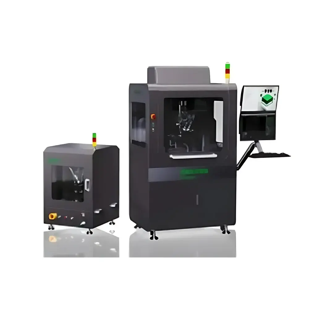
The Enovate3D Precision Series EP400-FP is a microscale additive manufacturing platform engineered for high-fidelity fabrication of functional electronic structures in semiconductor packaging, RF/microwave device prototyping, and advanced interconnect development. Unlike conventional laser-powder bed fusion or stereolithography systems, the EP400-FP employs precision direct ink writing (DIW) — a contactless, nozzle-based extrusion process operating under laminar flow control — to deposit functional nanomaterial inks with sub-micron placement accuracy. Its core architecture integrates piezoelectric-driven microdispensing, active thermal management of ink rheology, and closed-loop motion control with <±100 nm positional repeatability over 300 × 300 × 50 mm³ build volume. Designed specifically for R&D labs and pilot-line fabs, the system bridges the gap between photolithographic patterning and freeform 3D structuring — enabling rapid iteration of antenna geometries, redistribution layer (RDL) architectures, embedded passive components, and conformal flexible circuits without mask tooling or vacuum infrastructure.
Key Features
- Sub-10 µm feature resolution: Achieves consistent line widths down to 1 µm using proprietary silver, copper, and nickel nanoparticle inks formulated for low-temperature sintering (<150 °C) and high conductivity (>20% IACS after post-processing).
- Modular multi-process integration: Standard DIW module supports seamless coupling with optional in-chamber modules — including CNC-guided mechanical micro-drilling (±0.5 µm tool positioning), UV/IR laser ablation (spot size <5 µm, pulse duration <10 ns), and in-situ diode-laser sintering (power-adjustable 1–20 W, real-time pyrometric feedback).
- Multi-material co-printing capability: Equipped with up to six independently controlled fluidic channels, each with pressure-regulated dispensing and temperature-stabilized reservoirs (20–80 °C range), enabling graded composites, insulator-conductor stacking, and heterogeneous dielectric-metal lamination.
- Quick-swap print head system: Interchangeable nozzles (1–50 µm orifice diameters) mount via ISO-standard kinematic interface; full head replacement completed in <90 seconds without recalibration.
- Environmental enclosure: Class 1000 cleanroom-compatible chamber with HEPA filtration, inert gas purging (N₂ or Ar), and humidity control (30–50% RH) to ensure ink stability and prevent oxidation during printing.
Sample Compatibility & Compliance
The EP400-FP accommodates substrates ranging from silicon wafers (up to 200 mm diameter) and ceramic LTCC tapes to polyimide foils, glass carriers, and flexible PET films. Substrate flatness tolerance: ≤2 µm PV over 100 mm. Surface preparation protocols include O₂ plasma activation, HMDS vapor priming, and spin-coated adhesion promoters — all compatible with standard cleanroom workflows. The system meets ISO 14644-1 Class 7 environmental requirements when operated within certified enclosures. Software logs and hardware event timestamps comply with ALCOA+ principles (Attributable, Legible, Contemporaneous, Original, Accurate, Complete, Consistent, Enduring, Available) for GLP/GMP-aligned development environments. While not FDA-cleared as a medical device, its data integrity framework aligns with 21 CFR Part 11 expectations for electronic records and signatures when configured with audit-trail-enabled software licensing.
Software & Data Management
Controlled via Enovate3D’s proprietary PrecisionPrint Suite (v4.2+), the platform delivers parametric path planning, real-time ink viscosity compensation, and adaptive layer-by-layer calibration. CAD import supports STEP, IGES, and G-code (ISO 6983); native mesh processing includes automatic support generation for overhangs >45° and curvature-aware rasterization. All print jobs generate immutable JSON metadata bundles containing nozzle ID, ink lot traceability, environmental sensor readings (T/RH/O₂), motion trajectory logs, and image-captured layer verification (via integrated 5 MP coaxial microscope). Data export conforms to ASTM E2911-22 (Standard Guide for Digital Data Exchange in Additive Manufacturing) and supports automated transfer to LIMS or MES platforms via RESTful API or OPC UA interface.
Applications
- Radar and 5G/6G mmWave antenna arrays: Printed fractal, helical, and metamaterial unit cells on low-loss laminates (e.g., Rogers RO4000® series) with measured insertion loss <0.3 dB at 28 GHz.
- Advanced packaging interconnects: High-aspect-ratio TSV-like vias, fan-out RDLs, and bridge structures on 2.5D/3D IC substrates with <2 µm registration accuracy relative to lithographically defined pads.
- MEMS and sensor integration: Direct-write of strain-sensitive metallic traces on Si diaphragms, piezoresistive composites on polymer cantilevers, and embedded RF chokes in MEMS package lids.
- Flexible hybrid electronics: Multilayer circuitry on roll-to-roll compatible substrates, including stretchable antennas for wearables and conformal EMI shielding on curved surfaces.
- Prototyping of quantum device interconnects: NbTiN and Al superconducting traces printed on sapphire or high-resistivity silicon with critical current densities >1 MA/cm² post-annealing.
FAQ
What substrate materials are supported for high-resolution metal printing?
Silicon wafers (100–200 mm), alumina and aluminum nitride ceramics, polyimide (Kapton®), liquid crystal polymer (LCP), fused silica, and low-roughness FR-4 variants — all with surface roughness Ra <50 nm recommended.
Is the system compatible with industry-standard CAD and simulation tools?
Yes — native import of STEP/IGES geometry files and export of G-code compatible with Ansys HFSS, CST Studio Suite, and COMSOL Multiphysics for electromagnetic and thermal co-simulation.
Can print parameters be validated and documented for quality audits?
Every print job generates timestamped, digitally signed metadata packages meeting ALCOA+ criteria; optional IQ/OQ documentation kits available for regulated lab validation per ISO/IEC 17025.
What post-processing steps are typically required to achieve full electrical functionality?
Most conductive inks require thermal sintering (convection or laser-assisted) or photonic curing; sintering profiles are stored per ink lot and auto-loaded based on RFID-tagged cartridge identification.
Does the system support remote operation and monitoring in secure network environments?
Yes — TLS 1.2-encrypted remote desktop access, role-based user permissions, and syslog forwarding for SIEM integration are enabled via enterprise license tier.


