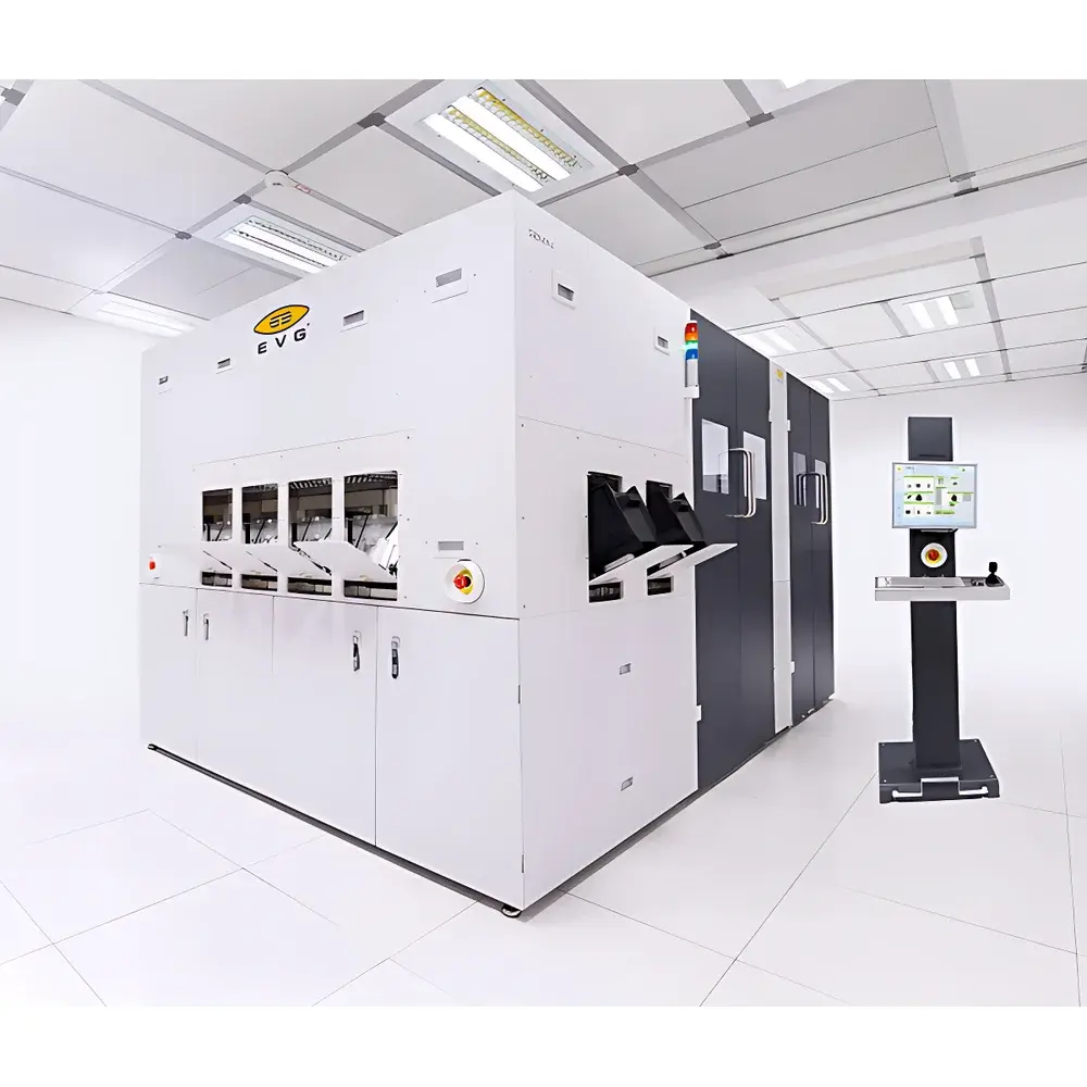
EV Group EVG Mask Aligner Series
| Brand | EV Group (EVG) |
|---|---|
| Origin | Austria |
| Manufacturer Type | Authorized Distributor |
| Product Origin | Imported |
| Model | EVG Mask Aligner Series |
| Exposure Mode | Proximity Mode |
| Resolution | ≥0.5 µm |
| Light Source | Mercury Arc Lamp |
| Wavelength | UV (i-line, g-line, h-line) |
| Illumination Uniformity | ±0.4% |
| Maximum Wafer/substrate Size | 2–8 inch (standard configuration) |
| Compatible Substrate Types | Si, SiC, GaAs, glass, quartz, flexible polymers |
| Alignment Accuracy | Sub-micron top-side and backside alignment |
| Vacuum Chuck Type | Pneumatic or electrostatic (model-dependent) |
Overview
The EV Group (EVG) Mask Aligner Series represents a foundational class of contact and proximity photolithography systems engineered for high-precision patterning in semiconductor R&D, pilot-line fabrication, and specialized microfabrication environments. Operating on the principle of proximity lithography—where a photomask is held at a controlled, non-contact gap (typically 10–50 µm) above the resist-coated substrate—the system leverages near-field optical projection to transfer patterned UV radiation onto photoresist layers. This approach avoids physical mask-substrate contact (eliminating mask damage and particle generation), while delivering robust resolution performance of ≥0.5 µm across standard wafer formats from 50 mm (2″) up to 200 mm (8″). First introduced with industry-defining innovations—including the world’s first bottom-side alignment system in 1985—EVG’s platform architecture integrates mechanical stability, thermal management, and optical homogeneity to ensure repeatable critical dimension (CD) control and overlay accuracy essential for advanced packaging, MEMS, compound semiconductors, and sensor development.
Key Features
- Proximity exposure mode with programmable gap control (10–50 µm) for optimized resolution vs. throughput trade-off
- High-intensity mercury arc lamp source delivering standardized i-line (365 nm), g-line (436 nm), and h-line (405 nm) UV spectra—compatible with broad-spectrum photoresists
- Optical illumination uniformity of ±0.4% across full exposure field, validated per ISO 9276-2 and ASTM E1753
- Multi-axis precision alignment stage supporting both top-side and bottom-side alignment with sub-micron repeatability (≤±0.25 µm)
- Modular vacuum chuck system accommodating rigid (Si, GaAs, quartz) and flexible substrates (polyimide, PET, metal foils) via pneumatic or electrostatic clamping
- Integrated process monitoring with real-time exposure dose control, lamp intensity feedback, and shutter timing calibration traceable to NIST-traceable radiometers
- CE-compliant mechanical design with interlocked safety enclosure, UV shielding, and ozone exhaust interface
Sample Compatibility & Compliance
EVG mask aligners accept substrates ranging from 2″ to 8″ in diameter (with optional upgrades to 300 mm), including silicon wafers, compound semiconductor blanks (GaAs, InP, SiC), fused silica masks, glass carriers, and thin-film polymer substrates. The system supports standard photoresists (e.g., AZ®, SU-8, ma-N) and lift-off processes without modification. All platforms are designed and verified in accordance with ISO 14644-1 Class 5 cleanroom compatibility requirements and meet IEC 61000-6-2 (immunity) and IEC 61000-6-4 (emissions) standards. Process documentation complies with GLP and GMP principles; audit trails, user access logs, and parameter change history are available for FDA 21 CFR Part 11–aligned validation packages upon request.
Software & Data Management
The EVG SmartView™ control software provides intuitive GUI-based operation with recipe-driven exposure sequencing, alignment map storage, and multi-layer registration logic. All exposure parameters—including dose (mJ/cm²), gap, alignment offset, lamp warm-up time, and focus compensation—are digitally logged with timestamp and operator ID. Data export supports CSV and XML formats compatible with MES integration (SEMI E10/E127 compliant). Optional software modules include automated alignment pattern recognition (using grayscale correlation algorithms), dose uniformity mapping, and SPC charting for Cp/Cpk analysis of exposure consistency over time.
Applications
- Advanced packaging: Redistribution layer (RDL) patterning, fan-out wafer-level packaging (FOWLP), and through-silicon via (TSV) lithography
- MEMS and sensors: High-aspect-ratio structures, inertial devices, pressure transducers, and optical MEMS mirrors
- Compound semiconductor manufacturing: GaN-on-Si HEMT patterning, LED mesa isolation, and photonic integrated circuit (PIC) waveguide definition
- Research & development: Rapid prototyping of microfluidics, plasmonic metasurfaces, and flexible electronics
- Academic and government labs: Teaching lithography fundamentals, process development, and cross-platform mask alignment benchmarking
FAQ
What wafer sizes does the standard EVG mask aligner support?
Standard configurations accommodate 2″, 3″, 4″, 6″, and 8″ substrates. Larger formats (up to 300 mm) require custom chamber and chuck assemblies.
Is backside alignment supported on all models?
Yes—bottom-side alignment capability is standard across the EVG 620, EVG 100, and EVG 200 series, enabling precise double-sided processing for through-wafer interconnects and stacked device architectures.
Can the system be integrated into an automated fab environment?
All current-generation EVG mask aligners feature SECS/GEM (SEMI E30/E37) and Ethernet/IP interfaces for host communication, tool status reporting, and remote diagnostics.
What UV wavelength options are available beyond standard mercury lines?
Custom broadband or narrowband LED-based illumination modules (365 nm, 385 nm, 405 nm) are available as factory-installed options for enhanced resist sensitivity and reduced thermal load.
Does EVG provide IQ/OQ/PQ documentation for regulated industries?
Yes—validated qualification packages including Installation Qualification (IQ), Operational Qualification (OQ), and Performance Qualification (PQ) protocols are available, fully aligned with ISO 9001, ISO 13485, and FDA 21 CFR Part 11 requirements.
Related Products


