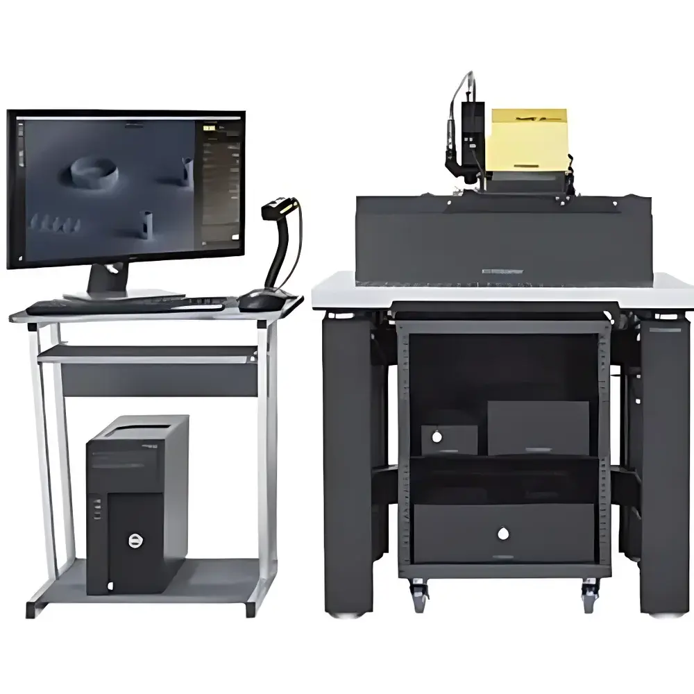
Exaddon CERES Micro/Nano Metal 3D Printing System
| Brand | Exaddon |
|---|---|
| Origin | Switzerland |
| Model | CERES |
| Laser Wavelength | 405 nm |
| Print Resolution | <1 µm |
| Max. Structure Height | 10 mm |
| Chamber Dimensions | 120 mm × 70 mm |
| Pressure Range | −800 to +1000 mbar |
| Bidirectional XY Repeatability | <500 nm |
| Printing Principle | Electrochemical Deposition (ECD) |
Overview
The Exaddon CERES Micro/Nano Metal 3D Printing System is a benchtop additive manufacturing platform engineered for sub-micrometer precision metal fabrication via localized electrochemical deposition (ECD). Unlike conventional laser-powder bed fusion or binder jetting systems, CERES operates without thermal input, eliminating melt pools, residual stress, and microcracking—enabling true bottom-up, layerless growth of freestanding metallic microstructures with nanoscale feature control. Designed for integration into cleanroom-compatible laboratory environments, the system delivers deterministic, maskless, direct-write metal patterning on conductive and non-conductive substrates—including silicon wafers, glass, polymers, and flexible electronics carriers. Its core architecture couples a high-precision piezo-driven nanopositioning stage with a microfluidic capillary probe capable of picoliter-scale electrolyte delivery and real-time current monitoring, ensuring stoichiometric control over Cu, Ni, Co, Pt, and Au deposits at deposition rates tunable from 102 to 105 atoms per second.
Key Features
- Sub-1 µm lateral resolution and <500 nm bidirectional XY repeatability across full 120 × 70 mm print chamber
- Electrochemical deposition-based process—no lasers, no sintering, no vacuum requirements—enabling ambient-air or controlled-atmosphere operation
- Integrated pressure-controlled microdispensing module (−800 to +1000 mbar) for stable meniscus formation and repeatable ion flux delivery
- Real-time amperometric feedback loop synchronized with stage motion for closed-loop thickness and composition control
- Modular probe design supporting interchangeable capillaries (inner diameters: 300 nm – 5 µm) for multi-material sequential printing
- Automated calibration routines for tip-substrate distance, electrolyte conductivity, and Faradaic efficiency compensation
Sample Compatibility & Compliance
CERES accommodates substrates up to 100 mm in diameter and 10 mm in thickness, including oxidized silicon, ITO-coated glass, PET films, and ceramic MEMS carriers. Surface preparation is minimal—native oxide layers serve as natural insulating barriers for selective deposition. The system complies with IEC 61000-6-3 (EMC emission standards) and meets CE marking requirements for laboratory instrumentation. While not classified as medical device or GMP-grade hardware, its data logging architecture supports audit-ready operation under GLP frameworks: all print parameters (voltage, current, pressure, position, timestamp) are recorded at ≥1 kHz sampling rate with SHA-256 hashed integrity verification. Optional firmware modules enable alignment with FDA 21 CFR Part 11-compliant electronic signatures and audit trails for regulated R&D environments.
Software & Data Management
The CERES Control Suite (v4.x) runs on Windows 10/11 and provides a Python API (PyCERES) for custom workflow automation. Design import supports G-code, SVG, and native .stl with voxel-based slicing optimized for ECD-specific constraints (e.g., minimum line width vs. charge density thresholds). All print jobs generate immutable HDF5 archives containing raw sensor streams, trajectory metadata, and post-processed 3D surface meshes. Data export options include standardized CSV (for statistical process control), TIFF stacks (for cross-sectional analysis), and STEP AP242 (for CAD-integrated metrology validation). Remote monitoring via TLS-secured WebSocket enables real-time status dashboards accessible from institutional intranets—no cloud dependency or external telemetry.
Applications
- Direct fabrication of plasmonic nanoantennas, RF metamaterial unit cells, and photonic crystal waveguides with <200 nm gap fidelity
- Prototyping of microelectrode arrays for neural probes, biosensors, and lab-on-chip interconnects
- In situ repair of defective traces on high-frequency PCBs and flex circuits without thermal damage
- Deposition of catalytic metal islands (e.g., Pt nanodots) for spatially resolved electrochemical scanning probe studies
- Hybrid fabrication: sequential printing of metal microcoils atop polymer MEMS actuators or piezoelectric thin films
- Calibration standards generation for SEM/EDS, AFM tip sharpening, and X-ray ptychography reference objects
FAQ
What metals can be printed using the CERES system?
CERES supports electrochemically depositable metals including copper, nickel, cobalt, gold, platinum, and silver alloys—subject to compatible aqueous or non-aqueous electrolyte formulations.
Is vacuum or inert gas required during printing?
No. The system operates under ambient laboratory conditions; optional glovebox integration is available for oxygen/moisture-sensitive electrolytes.
Can CERES print on non-conductive substrates?
Yes—via seed-layer sputtering or inkjet-printed conductive primers; the system includes protocols for galvanic nucleation initiation on dielectrics.
What is the typical throughput for a 5 µm × 5 µm copper pillar?
Approximately 4–6 seconds per pillar at 1 µm height, depending on current density and electrolyte conductivity.
Does the system support multi-material printing in a single run?
Yes—through automated probe exchange and electrolyte switching sequences programmed via the job scheduler.


