Freiberg Instruments MDPlinescan Online Carrier Lifetime Scanner for Wafer & Ingot Inspection
| Brand | Freiberg Instruments |
|---|---|
| Origin | Germany |
| Model | MDPlinescan |
| Sample Type | Monocrystalline & Multicrystalline Silicon Wafers, Ingots, and Processed Substrates |
| Measurement Principle | µ-PCD (Microwave Photoconductance Decay) & Steady-State Photoconductance |
| Carrier Lifetime Range | 0.1 µs – 10 ms (typ.) |
| Resistivity Range | 0.2 – 10³ Ω·cm |
| Conductivity Type | p-type & n-type |
| Sample Dimensions | Up to 50 × 50 mm² |
| Hardware Interface | Ethernet (TCP/IP, Modbus TCP) |
| Power Supply | 24 V DC, 2 A |
| Dimensions | 174 × 107 × 205 mm |
| Weight | 3 kg |
| Compliance | CE, RoHS, IEC 61000-6-2/6-4 |
| Software Protocol | Standard OPC UA & RESTful API support |
Overview
The Freiberg Instruments MDPlinescan is a compact, OEM-grade online carrier lifetime scanner engineered for real-time, non-contact characterization of silicon wafers and ingots in semiconductor manufacturing and photovoltaic production environments. It operates on the well-established principle of microwave photoconductance decay (µ-PCD), enabling quantitative mapping of minority carrier lifetime—directly correlated with bulk material quality, defect density, and recombination activity. Unlike destructive or offline metrology tools, the MDPlinescan delivers spatially resolved lifetime data at line speeds compatible with high-throughput production: full wafer scans completed in under one second. Its modular architecture supports both point-scan and area-scan configurations, making it suitable for inline process monitoring across crystal growth, wafering, surface passivation, diffusion, and metallization stages. The system requires no vacuum, no sample contact, and no consumables—only a stable 24 V DC power supply and standard Gigabit Ethernet connectivity.
Key Features
- Real-time µ-PCD-based minority carrier lifetime measurement with sub-millisecond temporal resolution and µs-level lifetime sensitivity
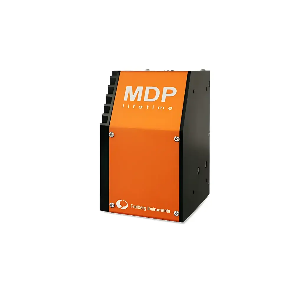
- OEM-optimized mechanical footprint (174 × 107 × 205 mm; 3 kg) designed for seamless integration into automated handling systems, conveyor lines, or robotic end-effectors
- Flexible excitation modes: pulsed laser (for µ-PCD) and steady-state illumination (for quasi-steady-state photoconductance), enabling dual-mode resistivity and lifetime correlation
- Native support for p-type and n-type silicon, including as-grown, textured, coated, and metallized wafers—compatible with Czochralski, float-zone, and cast multicrystalline substrates
- Standard industrial communication protocols: Ethernet-based TCP/IP, Modbus TCP, and optional OPC UA server for PLC and MES integration
- Robust optical head with integrated temperature stabilization and ambient light rejection—validated for operation in cleanroom Class 1000 and factory-floor environments
Sample Compatibility & Compliance
The MDPlinescan accommodates a broad range of silicon-based substrates, including monocrystalline and multicrystalline ingots (up to 50 × 50 mm² cross-section), sawn wafers (standard thicknesses 150–200 µm), and processed wafers with dielectric passivation layers (SiNx, Al2O3) or metal contacts. It is insensitive to surface reflectivity variations when operated in calibrated µ-PCD mode and does not require front-side metallization or ohmic contacts. All electrical and electromagnetic emissions conform to IEC 61000-6-4 (emission) and IEC 61000-6-2 (immunity) standards. The device bears CE marking and complies with RoHS Directive 2011/65/EU. While not certified for FDA-regulated environments, its data integrity features—including timestamped raw signal logging and deterministic trigger synchronization—support GLP-aligned process documentation workflows.
Software & Data Management
The MDPlinescan ships with Freiberg’s open-architecture control software suite, providing real-time lifetime visualization, statistical process control (SPC) charting, and configurable pass/fail thresholds per measurement zone. Raw µ-PCD decay curves, lifetime maps (2D heatmaps), and derived metrics (e.g., τeff, ρ, σ) are exportable in HDF5, CSV, and XML formats. The embedded web server enables remote configuration and live monitoring via standard browsers. For enterprise integration, RESTful API endpoints allow direct ingestion into SQL databases or cloud analytics platforms (e.g., AWS IoT Core, Azure Digital Twins). Audit trails—including user login events, parameter changes, and firmware updates—are retained locally with configurable retention periods, supporting ISO 9001 and IATF 16949 traceability requirements.
Applications
- Ingot qualification: Rapid screening of crystallinity uniformity and bulk defect distribution prior to wafering
- Wafer incoming inspection: High-speed verification of minority carrier lifetime specifications on PV or power device wafers
- Passivation process control: Quantitative assessment of SiNx/Al2O3 layer effectiveness via surface recombination velocity estimation
- Diffusion furnace monitoring: Detection of phosphorus or boron profile anomalies through lifetime gradient analysis
- Metallization QA: Identification of metal-induced recombination centers post-screen printing or plating
- OEM integration: Embedded use in multi-sensor inspection stations alongside PL, EL, or reflectance modules
FAQ
What measurement principle does the MDPlinescan use?
It employs microwave photoconductance decay (µ-PCD), a non-contact, non-destructive technique that measures the transient photoconductance response of silicon to pulsed laser excitation.
Can it measure wafers with anti-reflective coatings or metal layers?
Yes—its µ-PCD mode is largely insensitive to front-side optical modifications, provided the laser wavelength (typically 905 nm or 1064 nm) achieves sufficient absorption depth in the substrate.
Is calibration required between different wafer types?
A single reference wafer calibration suffices for routine operation across p/n-type, mono/multi-Si, and varying resistivity ranges; no per-sample recalibration is needed.
How is synchronization achieved with conveyor motion?
Via hardware TTL triggers from encoder signals or PLC pulse outputs—ensuring pixel-to-position registration accuracy better than ±0.2 mm at 1 m/s belt speed.
Does the system support 200 mm or 300 mm wafers?
The standard MDPlinescan head is optimized for ≤50 mm × 50 mm areas; larger formats require custom scanning stages or tiling strategies, available upon request.


