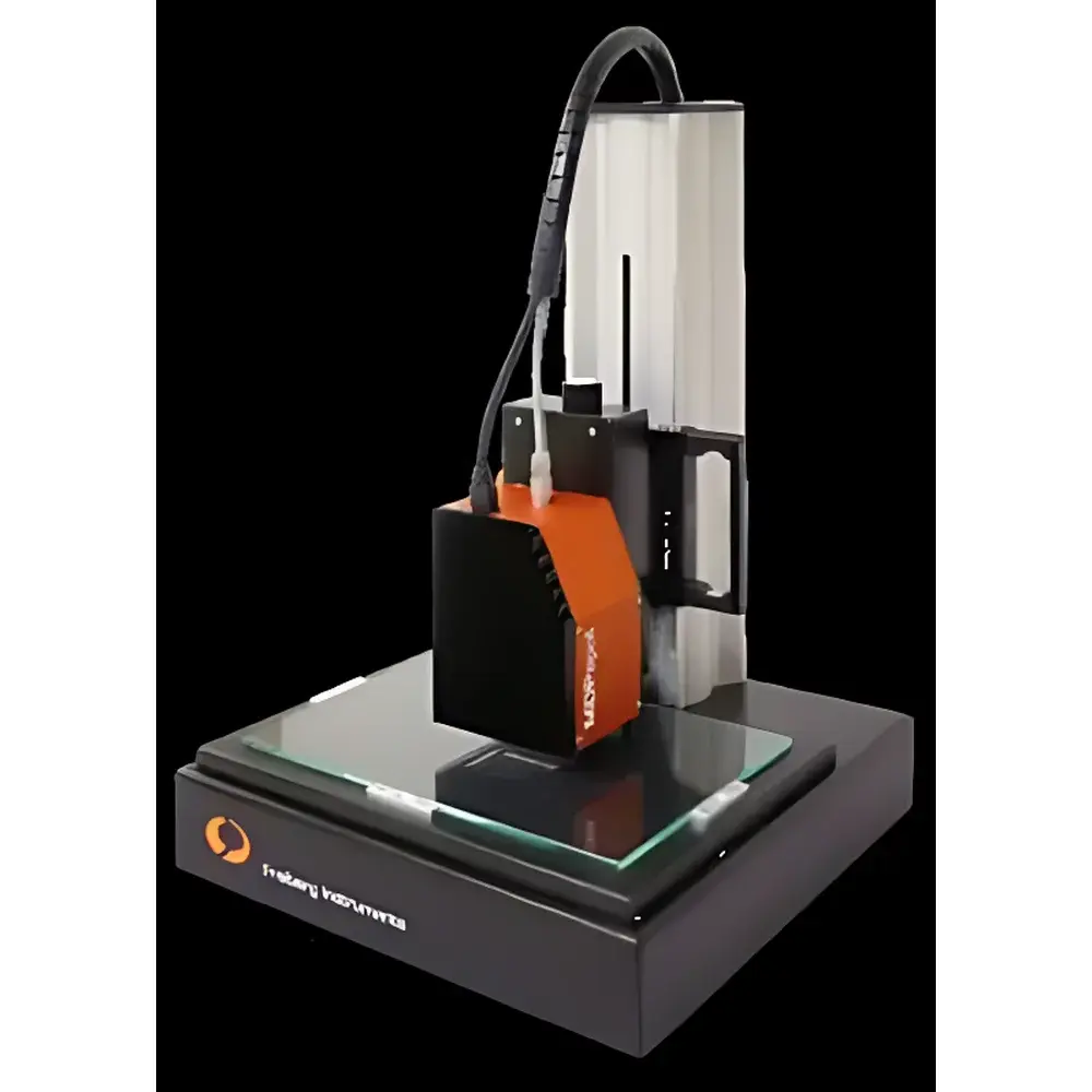
Freiberg Instruments MDPspot- Single-Point Minority Carrier Lifetime Tester
| Brand | Freiberg Instruments |
|---|---|
| Origin | Germany |
| Model | MDPspot- |
| Minority Carrier Lifetime Range | 20 ns to several tens of ms |
| Penetration Depth | 500 µm |
| Sample Size | min. 50 × 50 mm², max. 12″ (300 mm) or 210 × 210 mm² |
| Resistivity Range | 0.2 – >10³ Ω·cm |
| Compatible Materials | Silicon, compound semiconductors, oxides, wide-bandgap materials, perovskites, epitaxial layers |
Overview
The Freiberg Instruments MDPspot- is a high-precision, single-point minority carrier lifetime tester engineered for non-contact, non-destructive characterization of semiconductor materials. It operates on the principle of microwave-detected photoconductance decay (μPCD), combined with quasi-steady-state photoconductance (QSS-PC) and contactless resistivity mapping. This methodology enables quantitative evaluation of bulk recombination kinetics without surface passivation or electrical contacts—critical for process development, quality control, and failure analysis in photovoltaic and microelectronic manufacturing. The system delivers spatially resolved lifetime data at discrete measurement points across wafers, bricks, or heterostructured samples, supporting traceable metrology aligned with SEMI PV9-1110 and IEC 62788-1-2 standards for lifetime-based material qualification.
Key Features
- Single-point μPCD/QSS-PC dual-mode operation for high-fidelity lifetime extraction from sub-nanosecond to tens-of-milliseconds timescales
- Optimized microwave resonance cavity design ensuring >99.5% measurement repeatability and <±2% relative standard deviation across repeated acquisitions
- Modular benchtop architecture with industrial-grade thermal stabilization, achieving >99% uptime under continuous production-line conditions
- Motorized Z-axis stage with ±10 mm travel and 1 µm resolution for precise focus adjustment across variable sample topographies
- Integrated LED-based excitation source with tunable pulse width (10 ns–10 ms) and intensity control, compatible with low-injection and high-injection regimes
- IP-based remote interface compliant with IEEE 802.3 Ethernet standards, enabling secure web-accessible monitoring, diagnostics, and firmware updates
Sample Compatibility & Compliance
The MDPspot- accommodates diverse semiconductor geometries—from diced 50 × 50 mm² test coupons to full-size 300 mm (12″) wafers and 210 × 210 mm² square substrates used in tandem cell and perovskite module R&D. Its 500 µm effective optical penetration depth ensures representative bulk lifetime assessment in silicon wafers, GaAs epilayers, SiC substrates, metal oxide charge transport layers, and halide perovskite thin films. Resistivity mapping capability (0.2–>10³ Ω·cm) supports concurrent doping uniformity verification. All measurements comply with SEMI PV9-1110 requirements for minority carrier lifetime instrumentation, including calibration traceability to NIST-traceable reference samples and documented uncertainty budgets per ISO/IEC 17025.
Software & Data Management
Control and analysis are performed via the proprietary MDP Software Suite v4.x, a Windows-based application supporting automated measurement sequences, real-time decay curve fitting using multi-exponential models, and statistical process control (SPC) charting. Raw time-domain signals are stored in HDF5 format with embedded metadata (timestamp, excitation parameters, ambient temperature/humidity, operator ID). Audit trails meet FDA 21 CFR Part 11 requirements, including electronic signatures, user access levels, and immutable change logs. Export options include CSV, XML, and industry-standard SECS/GEM protocol integration for factory automation systems.
Applications
- Process validation of Czochralski and float-zone silicon crystal growth, including oxygen/carbon impurity correlation studies
- In-line monitoring of epitaxial layer quality in SiGe, GaN-on-Si, and AlGaN heterostructures
- Defect density mapping in kerfless wafering and laser grooving processes
- Stability assessment of perovskite absorber layers under thermal stress and illumination aging protocols
- Resistivity profiling across ion-implanted or diffusion-doped regions in power device substrates
- Qualification of recycled silicon feedstock and upgraded metallurgical-grade (UMG) silicon for PV applications
FAQ
What excitation wavelengths are supported?
The MDPspot- uses broadband visible/near-IR LEDs (centered at 660 nm and 940 nm) optimized for silicon and wide-bandgap materials; custom laser diodes (e.g., 405 nm for perovskites) can be integrated upon request.
Can the system perform spatial lifetime mapping?
While the MDPspot- is a single-point instrument, optional motorized XY stages enable automated point-by-point scanning to generate full-wafer lifetime maps with user-defined grid resolution.
Is calibration required between measurements?
No routine recalibration is needed; the system employs self-referencing microwave cavity resonance tracking and factory-calibrated photodetector gain tables, validated annually per ISO/IEC 17025 procedures.
Does it support p/n-type identification?
Yes—via contactless Hall-effect-assisted resistivity polarity detection, distinguishing p-type from n-type conduction in homogeneous and compensated materials.
How is data integrity ensured during remote operation?
All remote sessions use TLS 1.2 encryption, session timeouts, and dual-factor authentication; measurement data is write-protected at acquisition and digitally signed prior to export.


