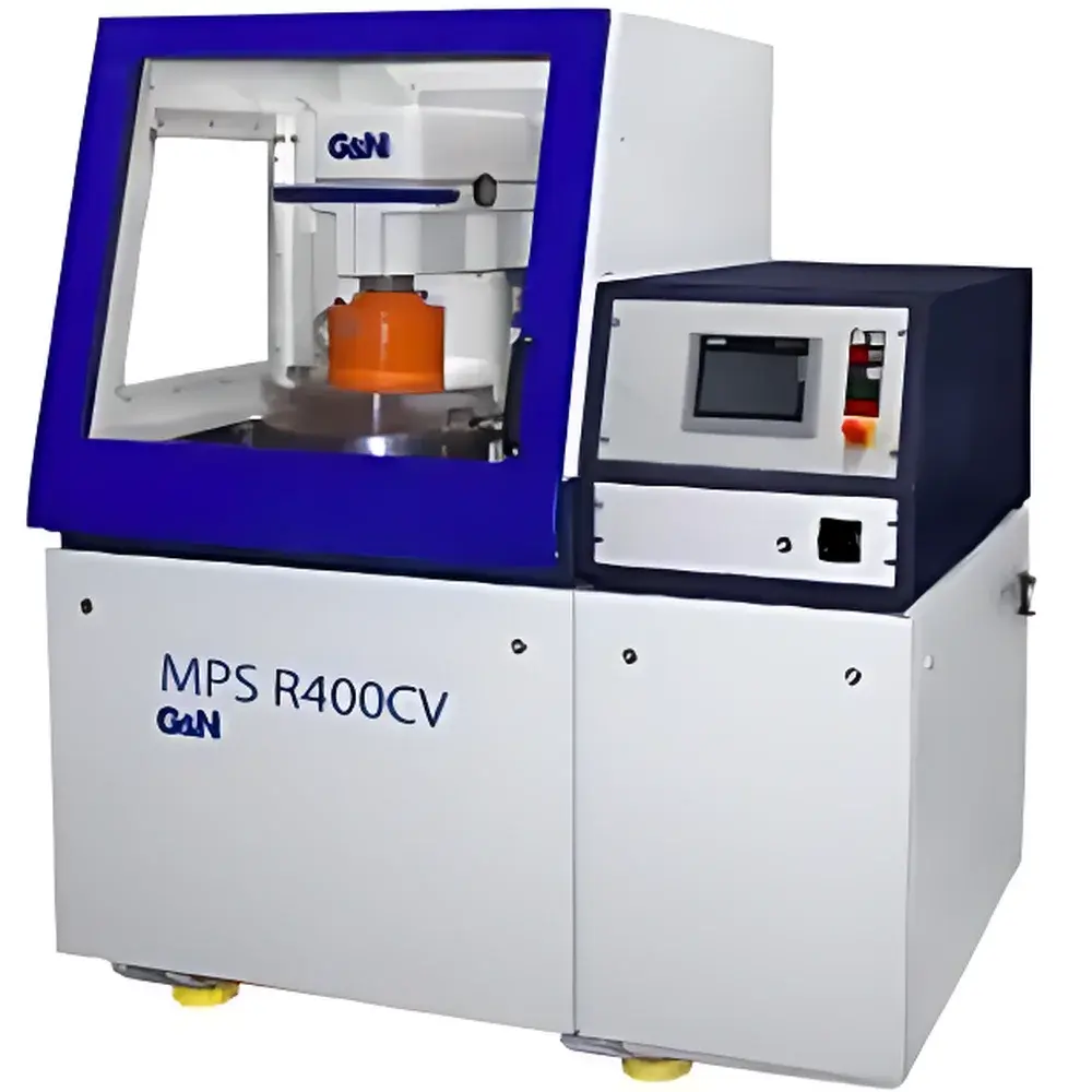
G&N MPS R400CV Wafer Grinding and Thinning System
| Brand | G&N |
|---|---|
| Origin | Germany |
| Model | MPS R400CV |
| Wafer Compatibility | 2″, 3″, 4″, 5″, 6″, 8″ |
| Chuck Flatness Error | ≤2 µm |
| Grinding Method | Z-axis plunge grinding with synchronized wafer and spindle rotation |
| Spindle Type | Integrated high-precision air-bearing spindle |
| Spindle Speed | 2560 rpm |
| Spindle Power | 3.7 kW |
| Grinding Wheel Diameter | 200 mm |
| Number of Spindles | 1 |
| Coarse/Fine Feed Range | 170 mm |
| Feed Resolution | ≤1 µm |
| Minimum Step Size | 0.1 µm |
| Coarse Grinding Rate | 2–1000 µm/min |
| Fine Grinding Rate | 2–1000 µm/min |
| Surface Roughness (Ra) | Down to 0.016 µm (with D7 diamond wheel) |
| Total Thickness Variation (TTV) | ≤3 µm per wafer |
| Inter-wafer Thickness Uniformity | ≤2 µm |
| Wheel Material | Diamond or CBN |
| Wheel Mounting | Single or dual-wheel configuration (manual or optional automatic change) |
| Chuck Sizes | Multiple vacuum chucks for 2″–8″ wafers |
| Sample Table Diameter | 400 mm |
| Sample Table Speed | 2–20 rpm |
| Control System | High-precision PLC-based controller with touchscreen HMI |
| Recipe Storage | Multiple programmable process recipes |
| Optional Module | In-situ thickness measurement unit |
| Enclosure | Fully enclosed grinding chamber |
| Machine Weight | 1130 kg |
| Footprint | 1640 × 1210 mm |
Overview
The G&N MPS R400CV Wafer Grinding and Thinning System is a precision-engineered platform developed by G&N GmbH — a German manufacturer with foundational expertise in semiconductor process equipment, tracing its lineage to Kugelmüller GmbH (founded 1940) and the world’s first commercial wafer grinder introduced in 1964. Designed for R&D laboratories and low-to-medium volume production environments, the MPS R400CV implements a vertical plunge grinding architecture based on air-bearing spindle technology and synchronized rotational kinematics between the wafer chuck and grinding wheel. This configuration ensures minimal thermal drift, high mechanical stability, and repeatable material removal rates across diverse substrate materials including Si, SiC, GaN, AlN, GaAs, InP, Ge, Al₂O₃, and Si₃N₄. The system operates under controlled environmental conditions within a fully enclosed grinding chamber, mitigating particulate contamination and enabling compliance with cleanroom-compatible workflows.
Key Features
- Air-bearing spindle with integrated 3.7 kW motor, delivering 2560 rpm nominal speed and sub-micron radial runout for high-fidelity surface generation.
- Z-axis plunge grinding mechanism with synchronized wafer rotation (2–20 rpm) and wheel rotation, ensuring uniform material removal and minimized edge chipping.
- Single-spindle design supporting either manual or optionally automated switching between coarse and fine diamond/CBN wheels (200 mm diameter), reducing setup time and cross-contamination risk.
- High-resolution servo-driven feed system with ≤1 µm positioning accuracy and 0.1 µm minimum step size, enabling precise control over depth-of-cut and layer-by-layer thinning protocols.
- Dynamically balanced chuck assembly with ≤2 µm flatness tolerance over 400 mm diameter, critical for achieving ≤3 µm TTV and ≤2 µm inter-wafer thickness deviation.
- Touchscreen-enabled PC-based HMI with intuitive recipe-driven operation; supports storage and recall of multiple grinding profiles, including speed, feed rate, dwell time, and wheel selection.
- Modular expandability: Optional in-line thickness metrology module enables real-time monitoring during grinding, facilitating closed-loop process control and endpoint detection.
Sample Compatibility & Compliance
The MPS R400CV accommodates wafers from 2″ to 8″ in diameter using interchangeable vacuum chucks. Its mechanical architecture and thermal management system are validated for use with brittle, anisotropic, and compound semiconductor substrates requiring stringent surface integrity and dimensional control. While the system itself does not carry CE marking for standalone medical device use, it conforms to EN 60204-1 (electrical safety), EN ISO 12100 (risk assessment), and EN 61496-1 (light curtain integration readiness). Process outputs meet typical requirements for backend packaging prep, MEMS fabrication, and power device manufacturing where adherence to JEDEC JESD22-A108 (temperature cycling) and SEMI F47 (voltage sag immunity) is expected at the facility level. Data logging functionality supports audit-ready traceability aligned with GLP principles.
Software & Data Management
The embedded PLC controller features deterministic real-time task scheduling and retains full process parameter history for each executed recipe. All operational events — including spindle activation, feed initiation, wheel contact detection, and emergency stops — are timestamped and stored locally. Export options include CSV-formatted logs compatible with LIMS integration and statistical process control (SPC) platforms. The HMI firmware supports user-level access control (operator, engineer, administrator) and maintains an immutable audit trail of parameter modifications, satisfying baseline requirements for FDA 21 CFR Part 11 Annex 11 alignment when deployed in regulated environments. No cloud connectivity is enabled by default; network interfaces are isolated unless explicitly configured per site-specific IT policies.
Applications
This system serves as a critical tool in advanced packaging development, particularly for fan-out wafer-level packaging (FOWLP), silicon photonics substrate preparation, and high-power semiconductor device thinning (e.g., SiC MOSFETs and GaN HEMTs). It is routinely employed to reduce wafer thickness to sub-100 µm while maintaining <3 µm TTV — a prerequisite for subsequent bonding, dicing, and testing steps. Academic and national lab users leverage its flexibility to investigate novel grinding chemistries, wheel topography effects on subsurface damage, and stress relaxation kinetics in wide-bandgap materials. Its compatibility with both conductive and insulating substrates also supports research into piezoelectric thin films (e.g., AlN on Si) and heterogeneous integration stacks.
FAQ
What wafer materials can be processed on the MPS R400CV?
Silicon (Si), silicon carbide (SiC), gallium nitride (GaN), aluminum nitride (AlN), gallium arsenide (GaAs), indium phosphide (InP), germanium (Ge), sapphire (Al₂O₃), and silicon nitride (Si₃N₄) are all supported, subject to appropriate wheel selection and process tuning.
Is the system suitable for cleanroom Class 100 or better environments?
Yes — the fully enclosed grinding chamber, filtered coolant recirculation (if equipped), and absence of oil-lubricated components enable safe deployment in ISO Class 5 (Class 100) cleanrooms when paired with facility-grade HEPA filtration and static-dissipative flooring.
Can the machine be integrated into a semi-automated production line?
Standard configurations include I/O ports compliant with SEMI E10 (equipment communications) and E30 (GEM) protocols; custom SECS/GEM interface development is available upon request.
What level of operator training is required?
A two-day onsite commissioning and operational training session is included with delivery, covering safety procedures, recipe creation, preventive maintenance, and basic troubleshooting — no prior grinding equipment experience is assumed.
Does G&N provide application support for new substrate materials?
Yes — G&N’s application engineering team offers remote and on-site process development assistance, including wheel specification guidance, parameter optimization studies, and surface characterization correlation reports.


