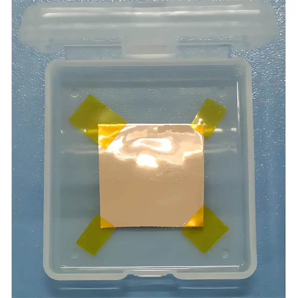
Graphene Film on Copper Substrate – Hefei Kejing Model
| Key | Purity: 99.95% |
|---|---|
| Cu Thickness | 50 µm |
| Sheet Resistance | 300–500 Ω/□ |
| Monolayer Coverage | ≥90–96% (size-dependent) |
| Layer Count | Single-layer or 2–4 layers |
| Substrate Dimensions | Custom up to 45 cm × 50 cm |
| Storage | Dry, oxygen-free environment, <30°C, use within 30 days |
Overview
Graphene film on copper substrate is a foundational two-dimensional material platform engineered for research and development in nanoelectronics, optoelectronics, flexible electronics, and fundamental condensed matter physics. This product utilizes chemical vapor deposition (CVD) to grow high-quality graphene directly on high-purity (99.95%) electrolytic copper foil (50 µm thick), followed by controlled transfer-ready preparation. The copper substrate serves as both catalytic growth surface and temporary mechanical support—enabling scalable, uniform monolayer or few-layer graphene synthesis with minimal grain boundary density and low defect concentration. Unlike exfoliated or solution-processed variants, CVD-grown graphene on Cu offers superior lateral continuity, reproducible electrical properties, and compatibility with wafer-scale fabrication workflows.
Key Features
- High-purity copper substrate (99.95% Cu) ensures minimal catalytic impurity incorporation during CVD growth, reducing dopant-induced carrier scattering.
- Controlled monolayer coverage of ≥90–96%, verified by Raman spectroscopy (G/2D intensity ratio ≈ 0.5–0.7, full-width-at-half-maximum (FWHM) of 2D peak < 30 cm⁻¹) and scanning electron microscopy (SEM) imaging.
- Consistent sheet resistance in the range of 300–500 Ω/□ across standard formats (2 cm × 2 cm to 12 cm × 20 cm), indicating low inter-grain resistivity and high carrier mobility under ambient conditions.
- Available in both single-layer and 2–4 layer configurations, enabling comparative studies of interlayer coupling, stacking order effects, and band structure modulation.
- Scalable dimensions—from laboratory-standard 2 cm × 2 cm samples up to custom formats of 45 cm × 50 cm—supporting prototyping, thin-film device integration, and pilot-line process validation.
- Pre-characterized with standardized Raman mapping and SEM documentation provided per batch, supporting traceability and experimental reproducibility.
Sample Compatibility & Compliance
This graphene-on-copper product is intended for use in academic, governmental, and industrial R&D laboratories conducting materials characterization, device fabrication, and process development. It complies with standard handling protocols for air-sensitive 2D materials and aligns with best practices defined in ASTM D8102-21 (Standard Guide for Characterization of Graphene Materials) and ISO/IEC 17025:2017 (general requirements for competence of testing and calibration laboratories). While not certified for medical or aerospace end-use, its manufacturing and packaging adhere to cleanroom-compatible procedures. All batches are documented with lot-specific Raman spectra and optical micrographs to support GLP-aligned reporting and internal quality review.
Software & Data Management
No proprietary software is bundled with this physical material. However, raw characterization data—including Raman spectral files (.txt or .csv), SEM image stacks (.tif), and optical micrographs—are supplied digitally upon request and formatted for interoperability with common scientific analysis platforms (e.g., OriginLab, ImageJ/Fiji, Python-based Raman processing libraries such as PyMca or scikit-raman). Metadata includes acquisition parameters (laser excitation wavelength, grating, integration time), sample ID, growth date, and storage duration. For laboratories operating under FDA 21 CFR Part 11 or EU Annex 11 requirements, metadata can be delivered with timestamped digital signatures and audit-trail logs upon formal agreement.
Applications
- Transfer-free electrical transport measurements using in-situ four-point probe or micro-fabricated electrode arrays.
- Template-assisted growth of heterostructures (e.g., h-BN/graphene/Cu, MoS₂/graphene/Cu) for van der Waals stacked devices.
- Reference standard for calibrating Raman spectrometers and validating graphene identification algorithms.
- Substrate for roll-to-roll compatible metallization or etch-stop layers in flexible circuit patterning.
- Model system for studying oxidation kinetics, hydrogen intercalation, and interfacial charge transfer at metal–2D material interfaces.
- Baseline material in inter-laboratory comparison studies targeting ISO/IEC 17043 proficiency testing schemes for 2D material metrology.
FAQ
What is the recommended method for transferring graphene from the copper substrate?
Standard wet-transfer using PMMA-assisted etching in ammonium persulfate (APS) or FeCl₃ solutions is validated for this product. Transfer yield and defect density depend on etchant concentration, temperature, and rinse protocol—detailed SOPs are available upon technical inquiry.
Can I perform direct lithography on the graphene/Cu film without transfer?
Yes—electron-beam lithography and photolithography have been successfully demonstrated on this substrate. Note that Cu’s high thermal conductivity and reflectivity require optimized exposure dose and developer dwell time.
Is the graphene pre-doped or intentionally doped?
No intentional doping is applied. As-grown films exhibit p-type behavior due to atmospheric adsorbates; carrier type and density may be modulated via annealing, encapsulation, or gate dielectric integration.
How is batch-to-batch consistency ensured?
Each production run undergoes inline Raman spot-checking (≥5 positions per 10 cm²), sheet resistance mapping, and optical uniformity grading prior to release. Certificate of Analysis includes mean G-peak position, I₂D/I_G ratio distribution, and coverage histogram.
Do you provide non-disclosure agreements (NDAs) for joint development projects?
Yes—custom NDA templates compliant with U.S. and EU jurisdiction are available for collaborative R&D engagements involving process integration or co-development of application-specific variants.