Hakuto IBE-C Ion Beam Etcher by ACCRETECH (Tokyo Seimitsu)
| Brand | ACCRETECH (Tokyo Seimitsu) |
|---|---|
| Origin | Japan |
| Manufacturer Type | Authorized Distributor |
| Origin Category | Imported |
| Model | 20 IBE-C |
| Pricing | Upon Request |
Overview
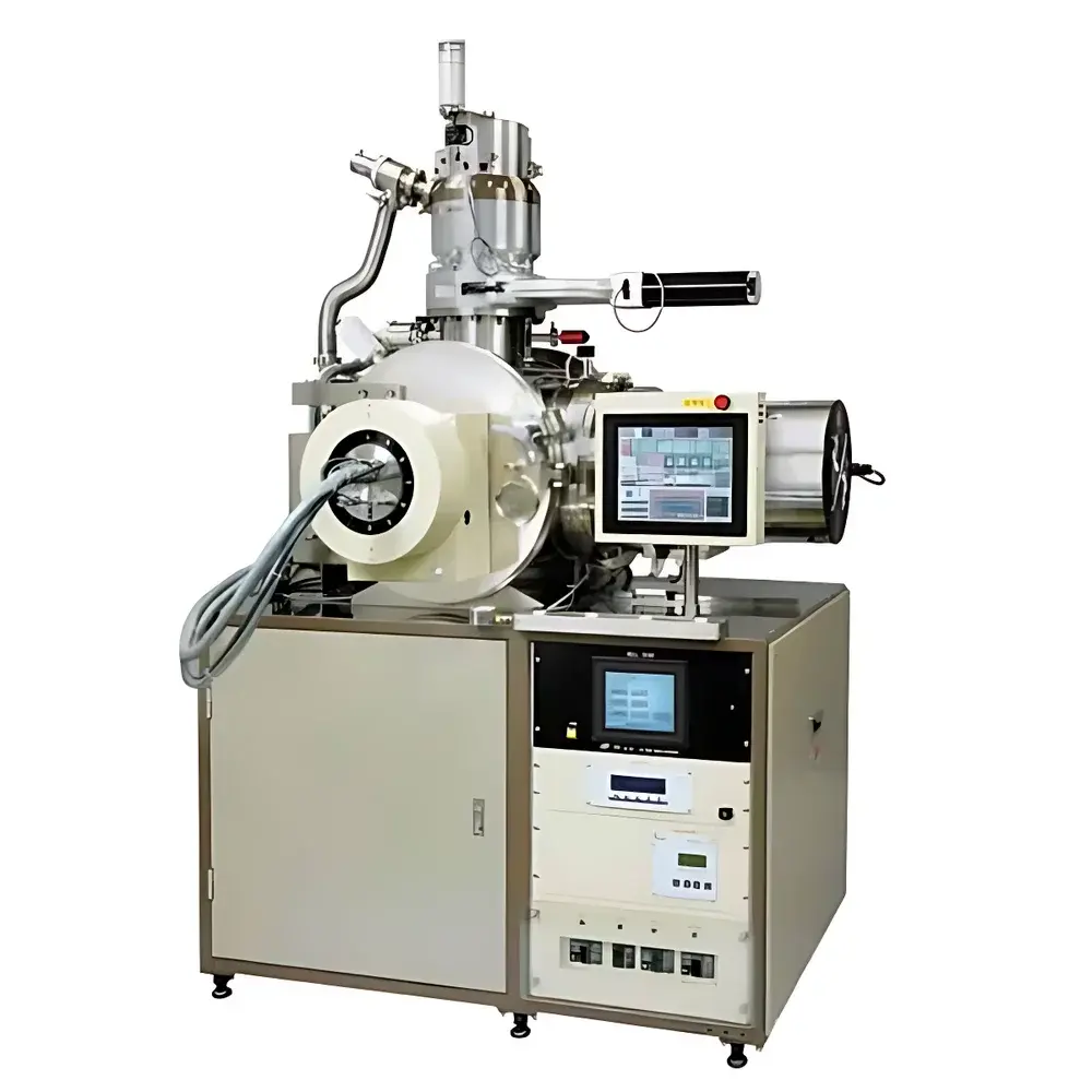
The Hakuto 20 IBE-C Ion Beam Etcher, engineered and manufactured in Japan by ACCRETECH (formerly Tokyo Seimitsu), is a high-precision physical dry etching system based on broad-beam ion beam sputtering. Unlike reactive ion etching (RIE) or plasma-based techniques, the IBE-C employs a collimated, low-energy (typically 0.5–2 keV) argon ion beam generated in ultra-high vacuum (UHV) conditions (<1×10⁻⁵ Pa base pressure). The beam is magnetically focused and electrostatically accelerated to produce a uniform, parallel flux of Ar+ ions that physically sputter target atoms from exposed surfaces—enabling highly anisotropic, non-chemical, and material-independent etching. This principle makes the system uniquely suited for applications where chemical selectivity, surface damage control, or etch-rate uniformity across dissimilar materials (e.g., magnetic multilayers, noble metals, oxides, nitrides, superconductors) are critical. Designed for R&D and pilot-line semiconductor fabrication, the IBE-C supports wafer diameters up to 300 mm (12″), with proven process stability across Si, GaN, LiNbO3, Pt, Au, NiFe, CoFeB, PZT, Ru, Ta, W, and complex heterostructures.
Key Features
- True Physical Etching Mechanism: Pure sputter-driven removal without reactive gases—eliminates polymer residues, undercut, or chemical contamination; ideal for clean interface engineering in spintronics and quantum devices.
- Adjustable Ion Incidence Angle: Ion source tilt mechanism enables precise beam alignment from –90° to +90° relative to substrate normal, supporting vertical sidewall definition, controlled profile tapering, and directional ion milling for TEM lamella preparation.
- Planetary Rotating Substrate Stage: Multi-axis synchronized rotation ensures exceptional etch uniformity ≤ ±5% across 4″, 6″, and 8″ wafers (≤ ±3% for optimized material/condition sets); validated per SEMI E10 and ISO/IEC 17025 traceable protocols.
- Dual Cooling Architecture: Direct water-cooled stage maintains substrate temperature <60 °C during extended etches; optional dry-type electrostatic chuck with metal-filled elastomer provides stable clamping and thermal coupling for temperature-sensitive films (e.g., YBCO, organic semiconductors).
- Modular Vacuum System: Configurable with Pfeiffer HiPace 800/1000 turbomolecular pumps and ACP series dry scroll backing pumps—achieving base pressures <5×10⁻⁶ Pa and enabling rapid pump-down (<30 min to operating pressure).
- Customization-Ready Platform: Fully configurable chamber geometry, stage size, ion source aperture, and load-lock integration—supporting manual, semi-automated, and fully automated (SEMI E40/E87 compliant) operation modes.
Sample Compatibility & Compliance
The IBE-C demonstrates broad compatibility with functional thin-film systems used in advanced semiconductor and microsystems research. It routinely processes magnetic tunnel junctions (MTJs), giant magnetoresistive (GMR) stacks, SQUID sensors, RF MEMS resonators, GaN HEMT gate recesses, LiNbO3 optical waveguides, and superconducting NbN/NbTiN circuits. Its non-reactive nature avoids fluorine- or chlorine-induced lattice disorder in compound semiconductors and preserves stoichiometry in piezoelectric oxides (e.g., AlN, PZT). The system meets key regulatory frameworks for lab instrumentation: vacuum integrity conforms to ISO 27417; electrical safety complies with IEC 61010-1; and operational logging supports GLP/GMP-aligned data integrity when paired with validated software (see below). While not FDA-certified as medical device hardware, its reproducibility and audit trail capability align with USP analytical instrument qualification (AIQ) requirements.
Software & Data Management
Control is managed via Hakuto’s proprietary Windows-based IBE-Soft v4.x platform, featuring real-time ion current monitoring, beam profile diagnostics, multi-step recipe management (with parameter locking per step), and automated endpoint detection via in-situ quartz crystal microbalance (QCM) or optical emission spectroscopy (OES) interfaces. All operational parameters—including beam voltage/current, stage temperature, chamber pressure, gas flow (if auxiliary gas inlet is installed), and etch time—are timestamped and stored in encrypted SQLite databases. Audit trails comply with 21 CFR Part 11 requirements when configured with electronic signatures, role-based access control, and immutable log archiving. Raw data export supports CSV, HDF5, and MATLAB-compatible formats for post-process analysis in MATLAB, Python (NumPy/Pandas), or JMP.
Applications
- Fabrication of high-resolution magnetic read/write heads and spin-transfer torque (STT) memory elements
- Defined edge structuring of superconducting quantum interference devices (SQUIDs) and Josephson junctions
- Surface cleaning and atomic-layer smoothing prior to epitaxial regrowth or bonding
- TEM sample preparation with minimal amorphization—especially for oxide heterostructures and topological insulators
- RF filter tuning via controlled thickness reduction of BST, AlN, or LiTaO3 resonator layers
- Micro-optical component patterning on nonlinear crystals (e.g., periodic poling of MgO:LiNbO3)
- MEMS inertial sensor release etching where isotropic undercut must be avoided
FAQ
What vacuum level is required for stable IBE operation?
The system achieves optimal beam stability and minimal background gas scattering at base pressures ≤5×10⁻⁶ Pa, attainable using the standard Pfeiffer turbomolecular pump configuration.
Can the IBE-C perform simultaneous etching and deposition?
No—the 20 IBE-C is a dedicated ion beam etcher. However, Hakuto offers hybrid IBE/PVD platforms (e.g., 30 IBE-PVD series) for sequential or in-situ etch/deposition processes.
Is remote diagnostics supported?
Yes—via optional Ethernet-connected VNC-enabled service port with TLS-encrypted remote access, allowing qualified field engineers to perform real-time troubleshooting and calibration verification.
What wafer handling options are available?
Manual loading (standard), semi-automated cassette-to-chamber transfer (with 25-wafer FOUP compatibility), and full cluster tool integration (SEMI E47.1 compliant) are all supported.
Does the system require special facility utilities?
Standard requirements include 208–240 VAC single-phase power, deionized cooling water (≤25 °C, 2–4 bar), and compressed dry air (≥6 bar, ISO 8573-1 Class 2). No hazardous gas lines or exhaust scrubbers are needed.


