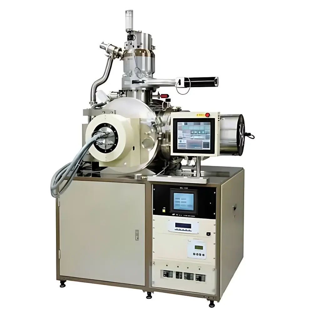
Hakuto by Pfeiffer Vacuum IBE-4000 Ion Beam Etching System
| Brand | ACCRETECH (Tokyo Seimitsu) |
|---|---|
| Origin | Japan |
| Manufacturer Type | Authorized Distributor |
| Origin Category | Imported |
| Model | Hakuto IBE-4000 |
| Pricing | Upon Request |
Overview
The Hakuto by Pfeiffer Vacuum IBE-4000 Ion Beam Etching System is a high-precision, physically driven dry etch platform engineered for nanoscale material removal with exceptional selectivity and surface integrity. Based on the fundamental principle of inert-gas ion sputtering—specifically using collimated, low-energy (0.1–2 keV) argon ion beams—the system achieves directional, non-reactive physical etching without plasma-induced damage or chemical residue. Unlike reactive ion etching (RIE) or inductively coupled plasma (ICP) systems, the IBE-4000 operates in ultra-high vacuum (UHV) conditions (≤5×10⁻⁷ mbar base pressure), enabling atomic-level control over etch rate, profile anisotropy, and interface sharpness. It is purpose-built for applications demanding minimal subsurface damage, stoichiometric fidelity, and compatibility with multilayer stacks containing dissimilar materials—particularly critical in spintronic device fabrication, magnetic sensor development, and RF MEMS packaging.
Key Features
- UHV-compatible chamber with all-metal seals and cryo-pumped base vacuum ≤5×10⁻⁷ mbar
- Collimated Ar⁺ ion source (Kaufman-type) with beam energy tunable from 100 eV to 2 keV and current density up to 1.2 mA/cm²
- Motorized, multi-axis sample stage with precise tilt (±15°), rotation (0–360°), and Z-height adjustment for uniformity optimization
- Integrated in-situ quartz crystal microbalance (QCM) for real-time etch rate monitoring and endpoint detection
- Support for wafer diameters up to 300 mm (12″), with standard configurations for 100 mm (4″), 150 mm (6″), and 200 mm (8″) substrates
- Etch uniformity ≤±5% across full wafer (≤±3% on selected materials such as NiFe, Pt, and Ru films)
- Modular design accommodating optional auxiliary sources (e.g., O₂ or CF₄ for hybrid ion-assisted etching)
Sample Compatibility & Compliance
The IBE-4000 demonstrates broad material compatibility—including ferromagnetic alloys (NiFe, CoFe, NiCo), noble metals (Au, Pt, Ru), piezoelectric oxides (PZT, LiNbO₃), compound semiconductors (GaN, GaAs), superconductors (YBCO), and insulating layers (SiO₂, Al₂O₃, Si₃N₄). Its physical sputtering mechanism eliminates concerns related to volatile byproduct formation, fluorine-induced corrosion, or plasma charging damage—making it ideal for delicate heterostructures used in MRAM, STT-MRAM, and quantum device research. The system conforms to ISO 14644-1 Class 5 cleanroom integration requirements and supports GLP-compliant operation through hardware-enforced interlocks, vacuum log archiving, and audit-trail-capable process recipe management.
Software & Data Management
Control is executed via the proprietary Hakuto IBE-OS v4.2 software suite, compliant with SEMI E30 (GEM) and E40 (SECS-II) standards for factory automation integration. All process parameters—including beam voltage/current, stage position/temperature, vacuum status, and QCM-derived etch depth—are timestamped and stored in SQLite-based local databases with configurable export to CSV or HDF5 formats. Full 21 CFR Part 11 compliance is enabled via optional electronic signature modules, role-based user access control, and immutable audit trails for recipe execution, maintenance logs, and calibration records.
Applications
- Thin-film magnetic head fabrication and pole tip trimming
- Spintronic stack patterning (e.g., CoFeB/MgO/Ta heterojunctions)
- MEMS resonator release and sidewall smoothing for high-Q RF filters
- Pt and Ti/Pt/Au electrode definition in thermal, IR, and strain sensors
- GaN-based laser diode facet etching and LN modulator electrode patterning
- Superconductor circuit lithography (e.g., Nb, NbN, YBCO) requiring zero chemical contamination
- TEM sample preparation via precision cross-sectioning and ion milling
FAQ
What distinguishes IBE from RIE or ICP etching?
IBE relies solely on physical sputtering using inert ions, eliminating chemical reaction pathways—thus avoiding residue, undercut, or plasma damage common in chemically assisted processes.
Can the IBE-4000 perform angled or shadow-mask etching?
Yes—its programmable tilt-and-rotate stage enables controlled off-normal incidence etching for sidewall engineering and lift-off compatible profiles.
Is remote diagnostics and preventive maintenance supported?
The system includes Ethernet-connected health monitoring with predictive alerts for ion source lifetime, pump performance degradation, and vacuum leak trends.
Does it support automated cassette-to-cassette wafer handling?
Fully integrated EFEM and cluster tool configurations are available under custom OEM agreements with ACCRETECH-certified robotics partners.
How is process reproducibility ensured across different labs?
Each system ships with NIST-traceable beam calibration certificates, standardized QCM reference films, and inter-lab validation protocols aligned with ASTM F2799-22 for ion beam etch rate metrology.
Related Products


