Hefei Kejing GaP (Gallium Phosphide) Single-Crystal Substrates for QCM and Electrochemical Sensing
| Brand | Hefei Kejing |
|---|---|
| Origin | Anhui, China |
| Manufacturer Type | Authorized Distributor |
| Product Category | Domestic |
| Model | GaP Single-Crystal Substrate |
| Pricing | Available Upon Request |
| Crystal Orientation | <100> (standard) |
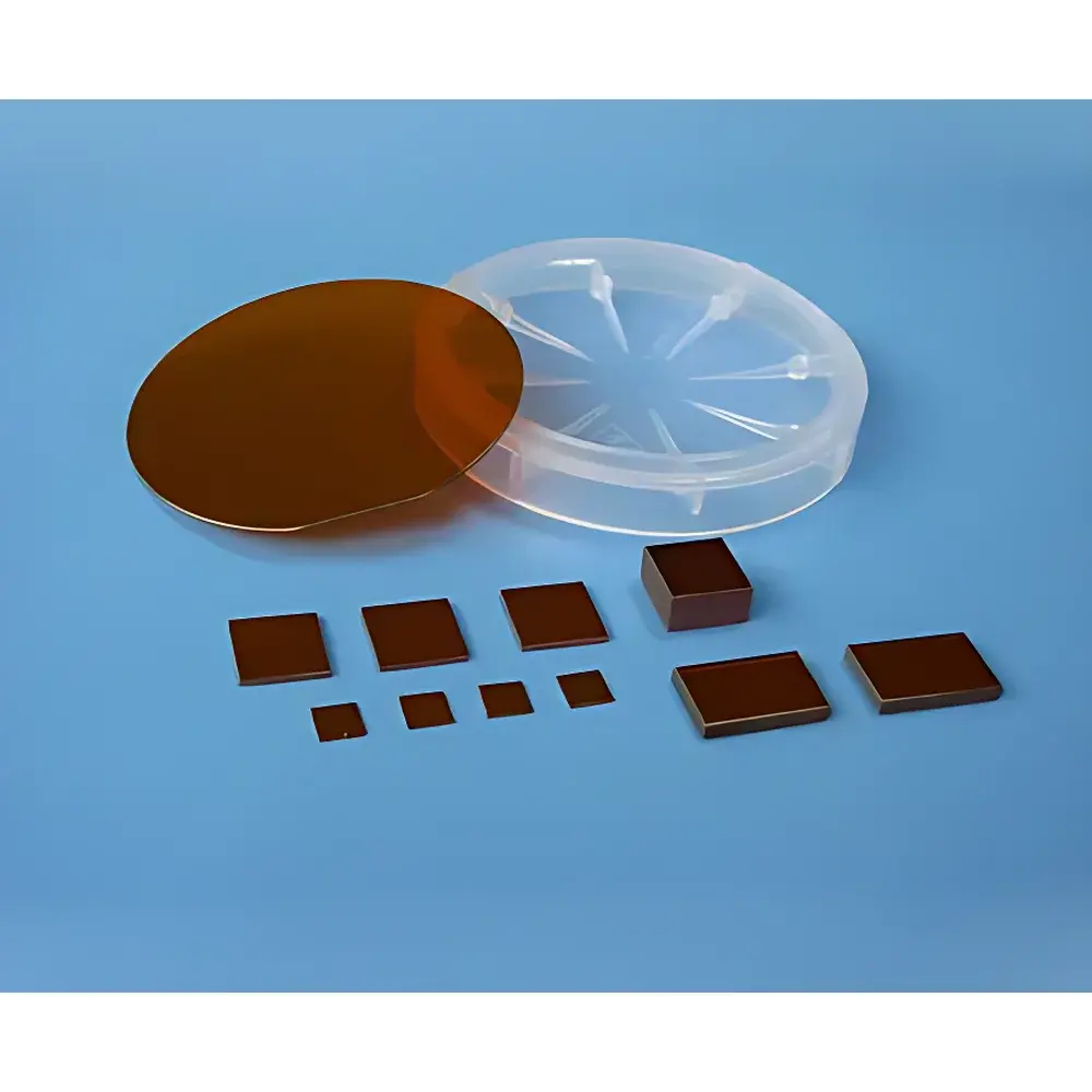
| Dimensions | 10 × 10 × 0.5 mm or Ø2" × 0.5 mm |
| Surface Finish | Single- or Double-Sided Polished |
| Surface Roughness (Ra) | <0.15 nm |
| Hardness (Mohs) | 3.0 |
| Density | 4.78 g/cm³ |
| Refractive Index | 3.45 |
| Elastic Modulus | 71 GPa |
| Growth Method | Liquid Encapsulated Czochralski (LEC) |
| Melting Point | 1072 °C |
| Carrier Concentration Range | 1×10¹⁶ – 6×10¹⁸ cm⁻³ |
| Dislocation Density | <5×10⁴ cm⁻² |
Overview
Hefei Kejing GaP (gallium phosphide) single-crystal substrates are engineered for high-stability resonant sensing platforms—particularly quartz crystal microbalance (QCM) systems requiring chemically inert, optically transparent, and electrochemically stable electrode supports. Unlike conventional quartz or SiO₂-based QCM crystals, GaP offers a unique combination of wide bandgap (2.26 eV), high thermal conductivity (110 W/m·K), and exceptional resistance to acidic and alkaline electrolytes—making it ideal for in situ electrochemical QCM (EQCM) studies where real-time mass change monitoring must coexist with aggressive redox environments. The substrate’s cubic zinc-blende lattice enables precise epitaxial integration with III–V semiconductor thin films and facilitates surface functionalization via well-established P–H or Ga–Cl surface chemistry. All wafers undergo rigorous post-growth annealing and are processed in ISO Class 3 (1000) cleanroom environments, then double-bagged in ISO Class 5 (100) cleanroom packaging to preserve atomic-level surface integrity prior to device fabrication.
Key Features
- High-purity single-crystal GaP wafers grown by Liquid Encapsulated Czochralski (LEC) method, ensuring low dislocation density (<5×10⁴ cm⁻²) and uniform carrier distribution
- Controlled doping options (undoped, Sn-, S-, Fe-, or Zn-doped) enabling tunable n-type conductivity across 1×10¹⁶ – 6×10¹⁸ cm⁻³
- Standard <100> crystal orientation optimized for consistent piezoelectric coupling and predictable acoustic wave propagation in thickness-shear mode (TSM) devices
- Double-side polished variants available with surface roughness Ra < 0.15 nm (measured by AFM), critical for minimizing scattering losses and enhancing Q-factor stability
- Thermally robust architecture: maintains structural integrity up to 500 °C in vacuum or inert atmospheres—compatible with RTP (rapid thermal processing) integration
- Customizable geometry: standard sizes include 10 × 10 × 0.5 mm and Ø2″ × 0.5 mm; custom orientations (<111>, <110>) and thicknesses (0.3–1.0 mm) available upon specification
Sample Compatibility & Compliance
GaP substrates are fully compatible with standard sputtering, e-beam evaporation, ALD, and MBE deposition tools used in thin-film QCM transducer fabrication. Their chemical inertness eliminates interfacial oxidation or hydrolysis during aqueous electrochemical testing—unlike GaAs or InP counterparts—which significantly improves long-term baseline drift performance. Each batch is supplied with a Certificate of Conformance documenting crystallographic orientation, surface flatness (≤0.5 µm TTV), and particulate count per SEM/EDS verification. While not certified to ISO 9001 at the wafer level, manufacturing adheres to GLP-aligned documentation protocols for traceability, including lot-specific growth logs, annealing profiles, and post-polish contamination screening (ICP-MS validated for Na, K, Fe, Ni, Cr ≤ 1×10¹⁰ atoms/cm²).
Software & Data Management
These substrates do not incorporate embedded electronics or firmware; however, they are designed for seamless integration into industry-standard QCM instrumentation platforms—including those compliant with ASTM E2551 (Standard Practice for QCM-Based Mass Measurement) and USP <1051> (Electrochemical Sensors). When paired with QCM-D (dissipation monitoring) systems, GaP’s high shear modulus (71 GPa) yields enhanced sensitivity to rigid film formation versus viscoelastic adsorption—enabling quantitative differentiation between monolayer chemisorption and multilayer physisorption events. Raw frequency shift (Δf) and dissipation (ΔD) data generated using GaP-based sensors are fully exportable in .csv and .txt formats for downstream analysis in MATLAB, Python (SciPy), or commercial packages such as QTools or Spreeta Suite.
Applications
- In situ monitoring of electrodeposition kinetics (e.g., Cu, Ni, Co) in sulfate- and chloride-based electrolytes
- Real-time detection of biomolecular binding (antibody–antigen, DNA hybridization) on carboxylated or amine-terminated GaP surfaces
- Stability assessment of protective coatings (e.g., polyaniline, PEDOT:PSS) under cyclic voltammetry stress
- Fundamental studies of solid–electrolyte interphase (SEI) evolution in Li-ion battery model systems
- Gas-phase sensing platforms integrating GaP with metal-oxide overlayers (e.g., SnO₂, WO₃) for ppm-level NH₃ or NO₂ detection
FAQ
What is the typical lead time for custom-oriented GaP substrates?
Standard <100>-oriented wafers ship within 5–7 business days. Custom orientations require additional LEC seed alignment and polishing validation, extending lead time to 3–4 weeks.
Can GaP substrates be used in HF-containing etchants?
Yes—GaP exhibits negligible etch rate in buffered HF (BHF) solutions (≤0.1 nm/min), unlike silicon or silica, making it suitable for selective release processes in MEMS-integrated QCM designs.
Is surface activation required before functionalization?
A brief O₂ plasma treatment (50 W, 60 s) is recommended to remove adventitious carbon and generate surface P–OH groups, improving silane or thiol monolayer uniformity.
Do you provide pre-patterned electrodes on GaP?
No—these are bare substrates. However, we supply technical notes on Au/Ti and Pt/Ti metallization recipes optimized for GaP adhesion and low-contact resistance.
Are certificates of analysis (CoA) available for each wafer lot?
Yes—CoAs include XRD rocking curve FWHM, secondary ion mass spectrometry (SIMS) dopant depth profiling, and AFM topography maps upon request.


")
