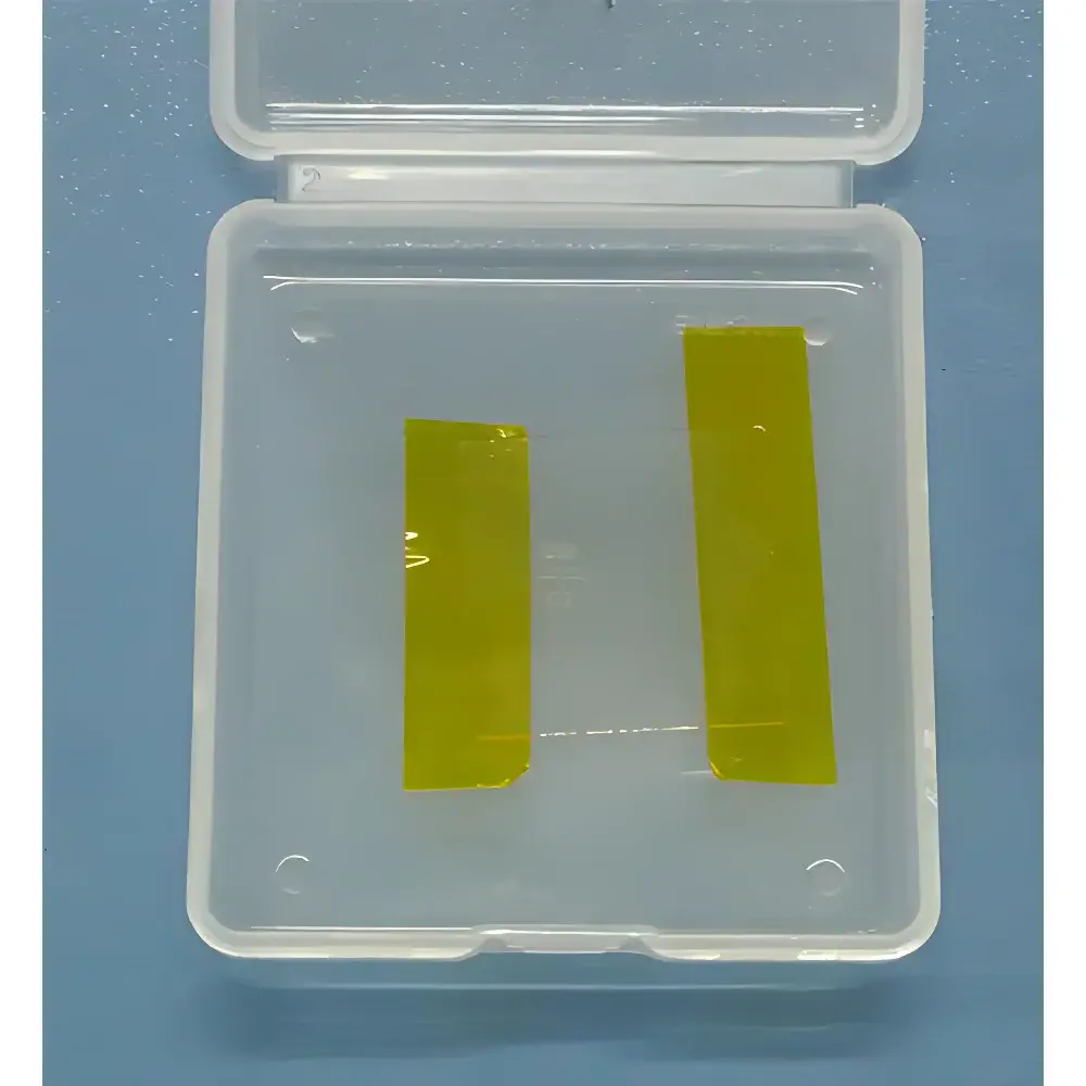
Hefei Kejing Quartz-Substrate Graphene Film
| Brand | Hefei Kejing |
|---|---|
| Origin | Anhui, China |
| Manufacturer Type | Authorized Distributor |
| Country of Origin | China |
| Model | Quartz-Substrate Graphene Film |
| Thickness | 1 mm / 2 mm |
| Quartz Transmittance | >93% (at 550 nm) |
| Sheet Resistance | 300–500 Ω/□ (monolayer), 200–300 Ω/□ (bilayer) |
| Monolayer Coverage | ≥95% |
| Available Sizes | 1 cm × 1 cm, 2 cm × 2 cm, 5 cm × 5 cm |
| Storage Condition | Dry, oxygen-free environment at <30 °C |
Overview
Hefei Kejing Quartz-Substrate Graphene Film is a high-performance optoelectronic material system engineered for applications requiring simultaneous optical transparency, electrical conductivity, and thermal stability. This product consists of chemical vapor deposition (CVD)-grown graphene transferred onto high-purity fused quartz substrates with controlled thickness (1 mm or 2 mm). The quartz substrate exhibits >93% transmittance across the visible spectrum (peak at 550 nm), enabling compatibility with UV-Vis spectroscopy, ellipsometry, and photonic device integration. Graphene layers—monolayer or bilayer—are verified via Raman spectroscopy and four-point probe measurements, delivering sheet resistances of 300–500 Ω/□ and 200–300 Ω/□ respectively, with monolayer coverage consistently exceeding 95% across all standard dimensions (1×1 cm², 2×2 cm², and 5×5 cm²). Unlike polymer-supported graphene films, this quartz-based architecture eliminates organic residue, minimizes interfacial scattering, and withstands thermal cycling up to 400 °C in inert atmospheres—making it suitable for vacuum-compatible thin-film processing, in situ characterization, and high-stability sensor platforms.
Key Features
- Optically transparent fused quartz substrate with certified transmittance >93% at 550 nm and low autofluorescence
- CVD-grown graphene with controlled layer count (monolayer or bilayer), confirmed by G/2D peak intensity ratio and full-width-at-half-maximum (FWHM) analysis in Raman spectra
- Uniform sheet resistance distribution (±8% spatial variation) measured by linear four-point probe mapping
- No polymeric transfer residues—quartz substrate enables direct integration into UHV chambers, sputtering systems, and atomic layer deposition (ALD) reactors
- Thermally stable up to 400 °C under N₂ or Ar; compatible with annealing protocols for defect healing and carrier mobility enhancement
- Available in three standardized formats (1×1 cm², 2×2 cm², 5×5 cm²) with documented batch-specific Raman and conductivity certification reports
Sample Compatibility & Compliance
This graphene film is designed for research-grade use in academic, national laboratory, and industrial R&D settings. It complies with standard cleanroom handling protocols (ISO Class 5 or better) and is packaged in nitrogen-purged, electrostatic-dissipative containers with oxygen scavengers. While not certified to ISO 9001 or IECQ QC 080000 as a finished electronic component, each batch undergoes in-house metrological validation aligned with ASTM E2524 (Standard Practice for Raman Microspectroscopy of Carbon Nanomaterials) and ISO/IEC 17025 traceable resistance calibration. The quartz substrate meets USP <381> specifications for optical-grade fused silica, ensuring minimal hydroxyl absorption and low thermal expansion coefficient (5.5 × 10⁻⁷ /°C).
Software & Data Management
Each shipment includes a digital Certificate of Conformance (CoC) containing batch ID, Raman spectral metadata (laser excitation wavelength, acquisition time, objective magnification), sheet resistance maps (ASCII grid format), and transmittance curves (CSV). No proprietary software is required—data files are compatible with common scientific analysis environments including MATLAB, Python (NumPy/Pandas), and OriginLab. For GLP/GMP-aligned workflows, raw measurement logs can be exported to support 21 CFR Part 11-compliant audit trails when integrated with validated LIMS platforms.
Applications
- Transparent conductive electrodes for OLEDs, perovskite solar cells, and flexible optoelectronics
- Substrate for in situ TEM/SEM studies of 2D material growth, interfacial reactions, and electrochemical processes
- Reference standard for calibrating graphene quality metrics (e.g., defect density, doping level, carrier mobility)
- Active layer in surface-enhanced Raman spectroscopy (SERS) substrates and plasmonic hybrid devices
- Platform for gated transport measurements in cryogenic Hall effect and quantum Hall regime experiments
- Model system for studying van der Waals heterostructure assembly and interlayer coupling dynamics
FAQ
What is the recommended storage environment for long-term stability?
Store in a dry, oxygen-free container (e.g., glovebox with <0.1 ppm O₂ or sealed desiccator with oxygen scavenger) at temperatures below 30 °C. Avoid exposure to ambient humidity, UV light, or mechanical abrasion.
Can these films be used directly in electron-beam lithography?
Yes—quartz substrates are electron-transparent at 100 keV and exhibit negligible charging. Graphene integrity remains intact during standard PMMA resist spin-coating and development when processed under inert conditions.
Is the graphene layer doped, and what is its typical carrier concentration?
As-supplied films exhibit p-type doping from atmospheric adsorbates (H₂O/O₂), yielding hole concentrations of ~1–3 × 10¹² cm⁻². Annealing at 200 °C in Ar/H₂ restores near-intrinsic behavior with carrier mobility >2,500 cm²/V·s (verified by field-effect transistor configuration).
Do you provide custom sizes or alternative substrates (e.g., CaF₂, sapphire)?
Custom dimensions up to 10 × 10 cm² and alternate substrates—including IR-transmissive CaF₂ and lattice-matched c-plane sapphire—are available under OEM agreement with minimum order quantities and extended lead times.
How is graphene layer continuity verified across larger areas (e.g., 5 × 5 cm²)?
Continuity is assessed via multi-point Raman mapping (100 µm step size) and statistical percolation analysis of sheet resistance uniformity; regions exhibiting >95% monolayer coverage meet specification thresholds defined in ASTM D7904 for 2D material homogeneity.