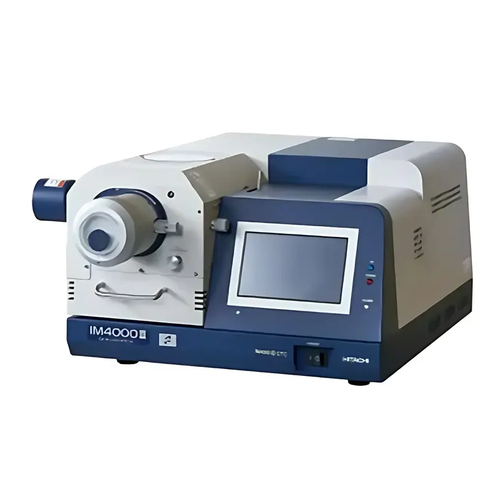
Hitachi IM400II and ArBlade 5000 Ion Milling Systems
| Brand | Hitachi |
|---|---|
| Origin | Japan |
| Model | IM400II / ArBlade 5000 |
| Sample Stage Cooling | Yes (Optional) |
| Vacuum Transfer Capability | Yes (Optional) |
| Dual-Stage Milling Mode | Yes |
| Touchscreen Interface | Yes |
| Maximum Cross-Section Width | 8 mm (±5 mm Traverse Range) |
| Ion Gun Configuration | PLUS Ion Gun (IM400II), PLUS II Ion Gun (ArBlade 5000) |
| Compliance | Designed for SEM/TEM sample preparation per ISO 14644-1 Class 5 cleanroom-compatible operation |
Overview
The Hitachi IM400II and ArBlade 5000 are high-precision ion milling systems engineered for reproducible, damage-minimized cross-sectional and planar sample preparation in semiconductor failure analysis, materials science, and advanced device characterization. Both instruments operate on the principle of broad-beam argon ion sputtering—where accelerated Ar⁺ ions impinge on a tilted specimen surface at controlled energy (typically 1–10 keV) and incidence angle, enabling deterministic removal of material with sub-nanometer depth resolution. Unlike mechanical polishing or FIB-based methods, ion milling avoids plastic deformation, smearing, or thermal artifacts, making it indispensable for preparing artifact-free interfaces in multilayer thin-film stacks, Cu/low-k interconnects, FinFET structures, and heterogeneous integration platforms. The IM400II serves as a versatile platform supporting both cross-section and planar milling modes, while the ArBlade 5000 extends performance with enhanced ion current density, optimized beam collimation, and expanded lateral traverse range—enabling uniform milling across 8 mm-wide sections without repositioning.
Key Features
- Simultaneous cross-sectional and planar milling capability via motorized dual-axis tilt and rotation stage
- Integrated cryogenic cooling stage (–120 °C to +50 °C) minimizes beam-induced heating, amorphization, and elemental redistribution in temperature-sensitive samples (e.g., organic semiconductors, phase-change alloys)
- Vacuum transfer interface compatible with Hitachi’s HTM series holders and third-party load-lock systems, ensuring contamination-free transfer to SEM, TEM, or XPS chambers under ≤1×10⁻⁶ Pa conditions
- PLUSTM and PLUS IITM ion gun architectures deliver stable, low-divergence beams with adjustable acceleration voltage (1–10 kV) and beam current (0.1–20 mA), enabling precise control over milling rate (0.1–50 nm/min) and surface roughness (Ra < 0.5 nm)
- Full-touch LCD control panel with intuitive workflow navigation, preloaded milling protocols, and real-time beam current/voltage monitoring
- Dual-stage automated milling sequence: coarse removal followed by fine finishing at reduced ion energy to suppress curtaining and redeposition
Sample Compatibility & Compliance
These systems accommodate wafers up to 200 mm diameter (with optional chucks), diced dies, TEM lamellae, and bulk specimens up to 30 mm × 30 mm × 10 mm. Compatible substrates include Si, SiC, GaN, sapphire, glass, polymers, and metal-ceramic composites. All vacuum components meet ISO 15732:2020 standards for residual gas analysis in ultra-high vacuum instrumentation. The integrated vacuum interlock system complies with IEC 61000-6-2/6-4 for electromagnetic compatibility, and operational software supports audit trail logging aligned with GLP and GMP documentation requirements per FDA 21 CFR Part 11 when paired with validated networked PC control.
Software & Data Management
Control is executed via Hitachi’s proprietary IonMill Manager™ software, running on Windows 10 IoT Enterprise. The interface supports protocol creation, parameter logging (time-stamped ion energy, current, pressure, stage position), and export of CSV-formatted process records. Email notification upon job completion is configurable via SMTP integration. Raw log files include metadata required for traceability in FA labs accredited to ISO/IEC 17025. Remote monitoring via Ethernet (TCP/IP) enables integration into centralized facility management systems without compromising data integrity.
Applications
- SEM/TEM cross-section analysis of BEOL interconnects, gate-all-around nanosheets, and 3D NAND vertical channel structures
- Interface characterization in heteroepitaxial layers (e.g., InP-on-Si, Ga₂O₃-on-sapphire)
- Failure root-cause analysis of delamination, void formation, and electromigration in advanced packaging (2.5D/3D IC, chiplets)
- Preparation of atom probe tomography (APT) specimens requiring sub-50 nm tip radii and minimal surface damage
- Planar thinning of brittle ceramics and MAX-phase materials for electron transparency
FAQ
What vacuum level is maintained during milling?
Base pressure is ≤5×10⁻⁵ Pa; operating pressure during sputtering ranges from 1×10⁻⁴ to 5×10⁻⁴ Pa, controlled via feedback-regulated turbomolecular pumping.
Can the system be integrated with an existing SEM chamber?
Yes—vacuum transfer modules support direct docking with Hitachi SU-series and Regulus-series SEMs using standard CF-63 or CF-100 flanges.
Is ion beam alignment user-adjustable?
Beam centering and focus are factory-optimized and locked; routine maintenance does not require realignment due to rigid ion gun mounting and differential pumping architecture.
What is the typical milling rate for silicon at 6 kV?
Approximately 15–25 nm/min under standard conditions (8 mm traverse, 7° incidence, 10 mA beam current); rate varies with crystallographic orientation and local topography.
Does the system support automated recipe import/export between instruments?
Yes—XML-based protocol files are portable across IM400II and ArBlade 5000 units, enabling method transfer consistency in multi-tool environments.
Related Products


