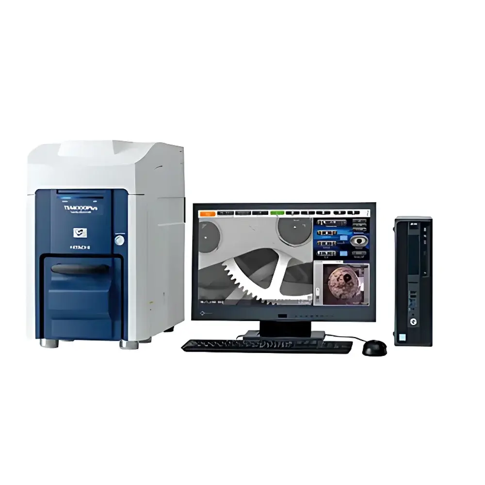
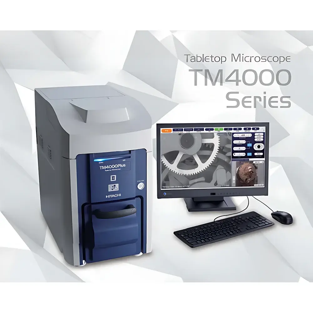
Hitachi TM4000II and TM4000PlusII Desktop Scanning Electron Microscope
| Brand | Hitachi |
|---|---|
| Origin | Japan |
| Model | TM4000II / TM4000PlusII |
| Accelerating Voltage | 5 kV / 10 kV / 15 kV (4-step current adjustment per voltage) |
| Magnification Range | 10× to 100,000× |
| Detector Configuration | Quad-segment backscattered electron detector (BSE) |
| Sample Chamber Dimensions | Ø80 mm × 50 mm (max. height) |
| Imaging Modes | Conductive mode (TM4000PlusII), Standard mode, Charge-free mode |
| Software Features | SEM-MAP navigation, report-generation export (PDF/HTML), real-time BSE + SE image overlay (TM4000PlusII) |
| Camera Resolution | 2560 × 1920 (CCD) |
| EDS Compatibility | Integrated EDX interface |
Overview
The Hitachi TM4000II and TM4000PlusII are compact, high-performance desktop scanning electron microscopes (SEM) engineered for rapid, high-fidelity imaging of non-conductive and beam-sensitive specimens without mandatory metal coating or complex vacuum preparation. Leveraging Hitachi’s proprietary low-vacuum operation (typically 10–130 Pa), these instruments enable stable electron beam interaction with hydrated, insulating, or outgassing samples—such as polymers, biological tissues, ceramics, and geological sections—while maintaining sub-10 nm effective resolution under optimal conditions. Unlike conventional high-vacuum SEMs requiring sputter-coating, the TM4000 platform operates with minimal sample modification, significantly reducing workflow latency and preserving native surface morphology. The system employs thermionic tungsten filament electron optics, optimized for consistent beam stability across three selectable accelerating voltages (5 kV, 10 kV, 15 kV), each supporting four discrete probe current settings to balance signal-to-noise ratio, depth of field, and charging mitigation.
Key Features
- Low-vacuum SEM architecture enabling direct observation of uncoated, non-conductive, and semi-volatile specimens
- Quad-segment backscattered electron (BSE) detector providing simultaneous angular contrast acquisition for compositional mapping and topographic differentiation
- TM4000PlusII-specific Ultra-Vacuum Detector (UVD): a high-sensitivity secondary electron (SE) detector optimized for low-vacuum environments, delivering enhanced surface detail and edge definition
- Real-time overlay capability (TM4000PlusII): synchronized acquisition and pixel-aligned fusion of SE and BSE signals to extract complementary structural and compositional information in a single frame
- Integrated SEM-MAP navigation software with tiled-image stitching, stage coordinate referencing, and automated region-of-interest (ROI) recall
- Large specimen chamber accommodating samples up to Ø80 mm in diameter and 50 mm in height—compatible with standard petri dishes, wafer fragments, and bulk metallurgical mounts
- Native EDX interface supporting third-party energy-dispersive X-ray spectrometers for elemental analysis without hardware modification
Sample Compatibility & Compliance
The TM4000II and TM4000PlusII support a broad spectrum of materials without conductive coating, including but not limited to: polymer films, pharmaceutical tablets, battery electrode cross-sections, soil aggregates, insect cuticles, and sintered oxides. The charge-free observation mode dynamically adjusts beam parameters to suppress electrostatic accumulation on insulators. All operational modes comply with ISO 16700:2016 (electron probe microanalysis — terminology and conventions) and align with ASTM E1508-21 guidelines for qualitative SEM imaging. Data acquisition logs—including kV, probe current, working distance, dwell time, and detector gain—are automatically embedded in exported image metadata, satisfying GLP audit requirements for traceability. Instrument firmware supports user-defined calibration protocols and password-protected method templates for regulated QC/QA environments.
Software & Data Management
Hitachi’s proprietary MAPS (Microscope Application Processing System) software provides intuitive, icon-driven control of acquisition, navigation, measurement, and reporting functions. All images are saved in TIFF format with embedded EXIF-style metadata (including timestamp, operator ID, instrument serial number, and acquisition parameters). Report generation exports structured PDF or HTML documents containing annotated images, scale bars, magnification metadata, and optional EDX spectral overlays. Software supports DICOM export for integration into laboratory information management systems (LIMS) and includes built-in tools for line profile analysis, particle size distribution (PSD) histogramming, and grayscale thresholding. Audit trail functionality records all user actions—including parameter changes, image annotations, and report exports—with timestamps and operator credentials, meeting FDA 21 CFR Part 11 electronic record integrity standards when deployed with validated IT infrastructure.
Applications
- Quality control of additive-manufactured metal parts: pore analysis, unmelted powder detection, and interlayer bonding assessment
- Failure analysis in electronics: solder joint voiding, delamination in PCB laminates, and contamination identification on die surfaces
- Materials science research: phase distribution in multiphase alloys, grain boundary characterization in nanocrystalline ceramics, and dispersion homogeneity in composite fillers
- Life sciences: cellular ultrastructure of freeze-dried biofilms, pollen morphology, and scaffold porosity evaluation for tissue engineering
- Geosciences: clay mineral textural classification, vesicle quantification in volcanic glasses, and authigenic mineral growth sequencing
- Forensics: fiber comparison, gunshot residue morphology, and toolmark surface replication fidelity assessment
FAQ
Can the TM4000II/TM4000PlusII operate without a dedicated cooling water supply?
Yes. Both models use air-cooled tungsten filaments and solid-state detector electronics, eliminating dependency on external chillers or recirculating coolants.
Is EDS integration plug-and-play or does it require hardware modification?
EDX detectors connect via standardized USB 3.0 and X-ray trigger interfaces; no internal chamber modification is required. Hitachi validates compatibility with Oxford Instruments, Thermo Fisher Scientific, and Bruker QUANTAX platforms.
What is the minimum detectable feature size under low-vacuum conditions?
Effective resolution is specimen- and condition-dependent; typical best-case performance yields ~8–12 nm detail visibility on gold-on-carbon reference standards at 15 kV and optimal working distance.
Does the system support automated particle analysis workflows?
Yes. MAPS software includes batch processing modules for threshold-based particle segmentation, circularity calculation, Feret diameter measurement, and statistical export to CSV for downstream statistical analysis.
Are software updates provided remotely, and how is version control managed?
Firmware and application updates are distributed via Hitachi’s secure customer portal. Each release includes SHA-256 checksums and revision-controlled changelogs compliant with ISO 9001 configuration management requirements.


