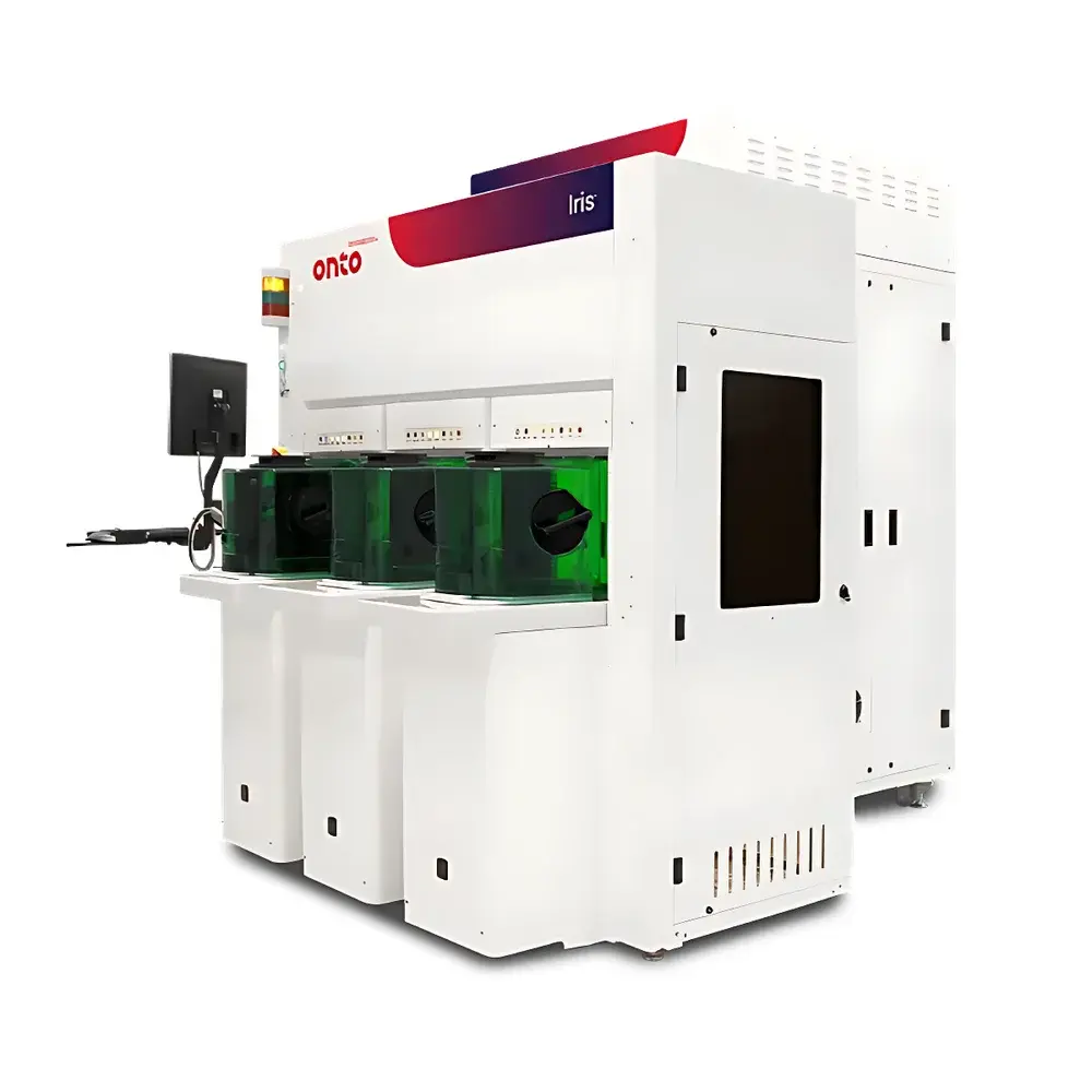
Onto IRIS S OCD and Thin-Film Metrology System
| Brand | AiYao Instruments |
|---|---|
| Origin | Malaysia |
| Manufacturer Type | Authorized Distributor |
| Origin Category | Imported |
| Model | IRIS S |
| Pricing | Available Upon Request |
Overview
The Onto IRIS S OCD and Thin-Film Metrology System is a semiconductor-grade, integrated optical metrology platform engineered for high-precision, non-destructive characterization of advanced process layers on silicon, SiC, GaN, and glass wafers. It combines spectroscopic ellipsometry (SE), Mueller matrix spectroscopic ellipsometry (MMSE), and spectral reflectometry (SR) within a single dual-channel optical architecture—operating across a broad spectral range from ultraviolet (UV) to near-infrared (NIR). The system implements oblique-incidence MMSE and normal-incidence SR simultaneously or independently, enabling robust decoupling of correlated optical parameters in complex multilayer stacks and periodic grating structures. Designed specifically for front-end-of-line (FEOL) and middle-of-line (MOL) process control, the IRIS S delivers sub-nanometer thickness resolution and high reproducibility for film metrology, critical dimension (CD) profiling, stress mapping, and composition analysis—including aluminum concentration quantification in doped films. Its compact footprint and modular design support integration into both R&D cleanrooms and high-mix production environments.
Key Features
- Dual-channel optical engine supporting concurrent MMSE (oblique incidence) and SR (normal incidence) measurements for enhanced parameter sensitivity and model stability
- Sub-nanometer measurement resolution for film thickness, CD profile, sidewall angle, and film stress—validated per SEMI MF1530 and ISO/IEC 17025 traceable protocols
- Automated wafer handling with dual-arm robotic loader, high-precision air-bearing stage, and adaptive autofocus enabling <100 ms per site positioning repeatability
- Full-wafer compatibility: supports 150 mm, 200 mm, and 300 mm substrates—including ultra-thin (100 µm bow), and bonded wafers
- Material-agnostic optical modeling: validated for Si, SiO₂, SiNₓ, low-k dielectrics, metal gates (TiN, TaN), III-V compounds (GaN, SiC), and transparent conductive oxides (ITO, AZO)
- SEMI-compliant automation interface (SECS/GEM) and Ai Diffract™ software suite with embedded audit trail, electronic signature, and 21 CFR Part 11–ready configuration options
Sample Compatibility & Compliance
The IRIS S accommodates standard and non-standard semiconductor substrates—including patterned and unpatterned wafers, SOI, epitaxial layers, and heterogeneous integration stacks. Its optical design mitigates scattering artifacts from rough surfaces and high-aspect-ratio features, ensuring stable fitting convergence for sub-10 nm gate oxide stacks and sub-20 nm fin profiles. All hardware and software components comply with SEMI S2/S8 safety standards and meet electromagnetic compatibility (EMC) requirements per IEC 61000-6-3. For regulated manufacturing environments, the system supports GLP/GMP-aligned workflows through configurable user roles, change control logs, and full data provenance tracking—including raw spectra, fit residuals, and covariance matrices archived in HDF5 format.
Software & Data Management
Ai Diffract™ is a physics-driven metrology software platform built on a model-guided machine learning framework. Rather than replacing first-principles optical modeling, it accelerates recipe development by intelligently suggesting initial parameter bounds, detecting degeneracy risks, and recommending optimal wavelength bands and incidence angles based on stack complexity. All measurement data—including time-stamped spectra, fitted layer models, and uncertainty estimates—are stored in a structured, queryable database compliant with ASTM E2948 metadata conventions. Batch reporting supports customizable PDF/Excel exports aligned with internal SPC templates and external fab MIS systems. Remote diagnostics and firmware updates are delivered via encrypted TLS channels with certificate-based authentication.
Applications
- Gate oxide and high-k dielectric thickness uniformity monitoring in CMOS logic and memory devices
- OCD-based CD, sidewall angle, and line-edge roughness (LER) extraction for EUV lithography process windows
- Stress mapping of tensile/compressive films (e.g., SiN capping layers) to predict warpage and delamination risk
- Aluminum concentration profiling in AlGaN barrier layers for power HEMTs and RF devices
- Multi-layer stack characterization in 3D NAND, DRAM capacitor stacks, and advanced packaging redistribution layers (RDL)
- Qualification of low-temperature ALD/CVD processes on flexible or thermally sensitive substrates
FAQ
Does the IRIS S support automated recipe transfer between tools in a multi-tool fleet?
Yes—Ai Diffract™ enables cross-platform recipe portability via standardized XML-based model definitions and spectral calibration reference files, fully compatible with Onto’s enterprise metrology management system (MMS).
Is the system qualified for use in FDA-regulated semiconductor manufacturing for medical device ICs?
Yes—the IRIS S can be configured with full 21 CFR Part 11 compliance, including role-based access control, electronic signatures, and immutable audit trails for all measurement and configuration events.
What level of training and application support is provided for new users?
Onto offers tiered support packages including on-site installation qualification (IQ/OQ), application-specific method development workshops, and quarterly remote calibration verification sessions conducted by certified metrology engineers.


