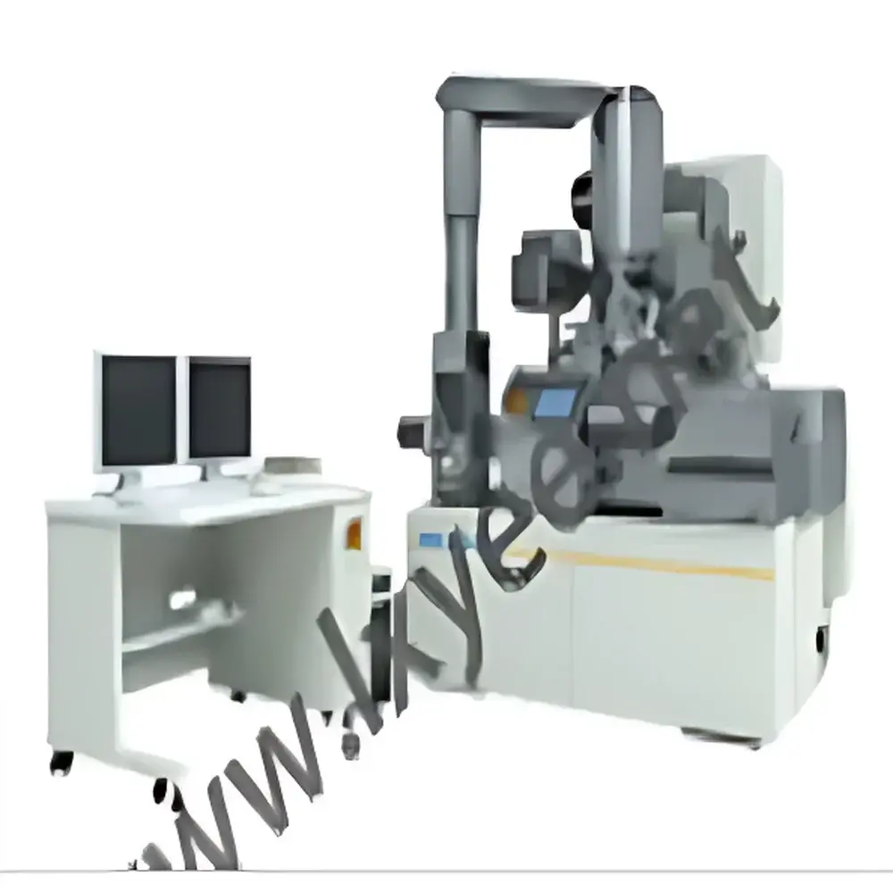

JEOL JBX-9500FS 100 kV Circular-Beam Electron Beam Lithography System
| Brand | JEOL |
|---|---|
| Origin | Japan |
| Model | JBX-9500FS |
| Acceleration Voltage | 100 kV |
| Maximum Substrate Size | 300 mm Ø wafers or 6-inch masks |
| Maximum Field Size | 1000 µm × 1000 µm |
| Stage Travel Range | 260 mm × 240 mm |
| Minimum Positioning Unit (LBC) | 0.15 nm (λ/4096) |
| Overlay Accuracy | ≤ ±11 nm |
| Field Stitching Accuracy | ≤ ±10 nm |
| In-Field Placement Accuracy | ≤ ±9 nm |
| Position DAC Resolution | 20-bit |
| Scan DAC Resolution | 14-bit |
| Scan Step Size | 0.25 nm |
| Maximum Scan Rate | 100 MHz |
| Electron Source | ZrO/W Schottky Emitter |
Overview
The JEOL JBX-9500FS is a high-performance, 100 kV circular-beam electron beam lithography (EBL) system engineered for nanoscale patterning in advanced R&D and pilot-line manufacturing environments. Operating on the principle of focused electron beam scanning in vacuum, the system delivers sub-10 nm placement fidelity across large-area substrates—enabling precise fabrication of photonic integrated circuits (PICs), DFB/DBR lasers, metamaterials, quantum device test structures, and nanoimprint master stamps. Its architecture integrates a thermally stable ZrO/W Schottky field-emission electron source with vector-scan and step-and-repeat writing modes, supporting both maskless direct-write and mask fabrication workflows. Designed for compatibility with semiconductor cleanroom infrastructure, the JBX-9500FS accommodates substrates up to 300 mm in diameter or 6-inch photomasks—making it one of the few EBL platforms capable of bridging academic nanofabrication requirements with industry-relevant wafer-scale process development.
Key Features
- 100 kV acceleration voltage enabling high-resolution, low-charging exposure of thick resist stacks and conductive substrates
- Circular-beam optics with vector-scan control and 100 MHz maximum deflection bandwidth for high-throughput patterning
- Laser-based stage positioning (LBC) achieving 0.15 nm minimum incremental motion (λ/4096 interferometric resolution)
- 20-bit position DAC and 14-bit scan DAC enabling 0.25 nm effective scan step size and <1 nm data fidelity reproduction
- Automated real-time correction algorithms for thermal drift, stage hysteresis, and beam landing shift—configurable per field, pattern, or time interval
- Integrated material cassette handling option (up to 10 cassettes) for unattended weekend operation under GLP-compliant logging
- Micro-pitch field tuning software for chirped grating fabrication (e.g., DFB laser waveguide gratings) with sub-nanometer period modulation
Sample Compatibility & Compliance
The JBX-9500FS accepts standard semiconductor substrates including silicon, SOI, InP, GaAs, SiC, and quartz wafers (up to 300 mm Ø), as well as fused silica and low-expansion glass photomasks (up to 6 inches). Its vacuum chamber and stage design conform to SEMI S2/S8 safety standards, while beam calibration protocols align with ISO/IEC 17025 traceability requirements for metrology-grade instrumentation. The system supports resist processing workflows compliant with JEOL’s recommended PMMA, ZEP, HSQ, and AR-P series chemistries—and its pattern placement accuracy meets critical requirements for NIST-traceable reference structure fabrication and EUV mask qualification support.
Software & Data Management
Controlled via JEOL’s proprietary LITHOGRAPHY STATION™ software suite, the JBX-9500FS provides full GDSII/OASIS import, hierarchical fracturing, proximity effect correction (PEC), and multi-pass dose modulation. All system parameters—including beam current, dwell time, focus offset, and stage trajectory—are logged with timestamped audit trails meeting FDA 21 CFR Part 11 and ISO 13485 electronic record integrity criteria. Data export supports standardized formats (e.g., CSV, HDF5) for integration into enterprise MES or FA systems. Optional networked remote monitoring enables secure access for cross-site collaboration without compromising local security policies.
Applications
- Fabrication of photonic crystal cavities, ring resonators, and silicon nitride waveguides for integrated photonics
- Direct-write of plasmonic nanoantennas and metasurface unit cells for sensing and beam shaping
- Production of high-fidelity diffractive optical elements (DOEs) and binary optical components
- Mask writing for nanoimprint lithography (NIL) templates used in OLED display and micro-LED transfer processes
- Quantum dot arrays, superconducting qubit test structures, and topological insulator device prototypes
- Calibration standards for CD-SEM, AFM, and scatterometry tools—traceable to NIST SRM references
FAQ
What is the smallest achievable feature size using the JBX-9500FS?
Feature resolution depends on resist chemistry, dose, and development—but the system routinely achieves sub-10 nm linewidths in high-resolution resists such as HSQ and ZEP520A under optimized conditions.
Does the system support automated alignment to pre-existing marks?
Yes. Integrated CCD-based mark recognition and closed-loop alignment enable overlay registration better than ±11 nm (3σ) to existing patterns on wafers or masks.
Is the JBX-9500FS compatible with existing cleanroom automation interfaces?
The platform supports SECS/GEM protocol integration and can be interfaced with factory host systems via Ethernet/IP or OPC UA for recipe management and status reporting.
How is beam stability maintained during extended write sessions?
Continuous active compensation—based on real-time interferometer feedback and beam landing monitors—corrects for thermal drift and mechanical relaxation over multi-hour exposures.
Can the system be configured for dual-beam or multi-column operation?
No. The JBX-9500FS is a single-column, high-current circular-beam platform optimized for precision rather than parallelization; JEOL offers separate solutions (e.g., JBX-6300FS) for multi-beam configurations.


