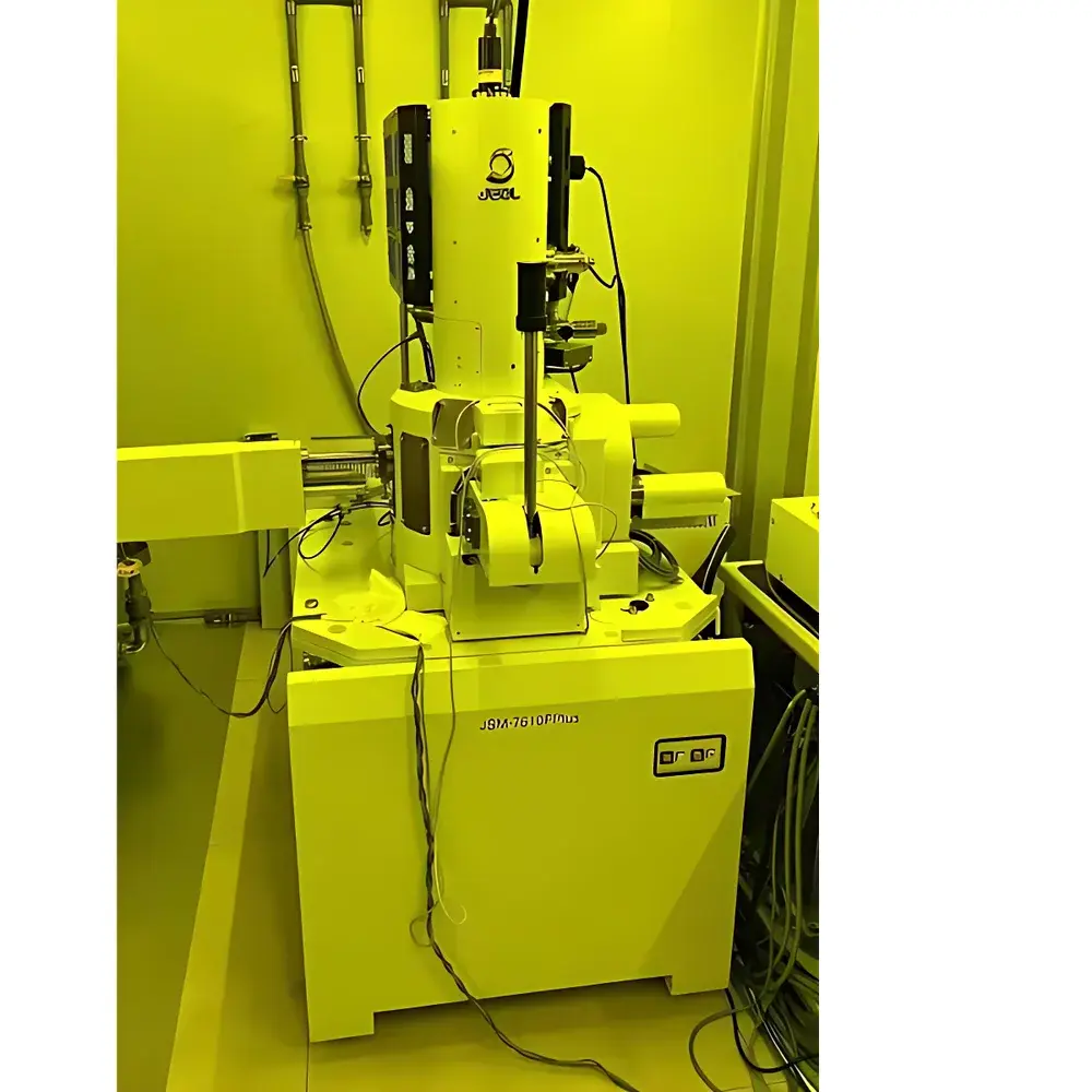
JEOL JSM-7610FPLUS Thermal Field-Emission Scanning Electron Microscope (SEM) with Integrated EDS and EBSD
| Brand | JEOL |
|---|---|
| Origin | Japan |
| Model | JSM-7610FPLUS |
| Year of Manufacture | 2017 |
| Operational Age | 5 years |
| Vacuum System | Turbo-molecular + Ion Pump |
| Max Magnification | 1,000,000× |
| Resolution (SE) | 0.8 nm @ 15 kV, 1.0 nm @ 1 kV |
| Acceleration Voltage | 100 V – 30 kV |
| Electron Source | Schottky Thermal Field-Emission Gun |
| Beam Current | Up to 200 nA |
| Working Distance | 8 mm |
| Stage | 5-axis Motorized, ±5° to +70° tilt, 360° rotation |
| EDS Detector Area | ≥20 mm², Be–Am detection range, Mn-Kα resolution ≤127 eV |
| EBSD Compatibility | Yes |
| Compliance | ASTM E1558, ISO 16700, IEC 61000-4-5 (EMC), GLP-ready data logging |
Overview
The JEOL JSM-7610FPLUS is a high-performance thermal field-emission scanning electron microscope (FE-SEM) originally commissioned in 2017 and operated for five years under controlled laboratory conditions. Engineered for nanoscale surface morphology characterization and microstructural analysis, it employs a Schottky-type thermal field-emission electron source coupled with an optimized strong-excitation objective lens design. This architecture delivers exceptional spatial resolution—0.8 nm at 15 kV and 1.0 nm at 1 kV in secondary electron (SE) mode—while maintaining beam stability and low-voltage imaging fidelity critical for insulating or beam-sensitive specimens. Its integrated In-Lens electron optics enable high-current operation (up to 200 nA) without compromising probe coherence, supporting demanding analytical workflows including energy-dispersive X-ray spectroscopy (EDS), electron backscatter diffraction (EBSD), and wavelength-dispersive spectroscopy (WDS). The system operates under ultra-high vacuum conditions (electron gun pressure <1×10⁻⁷ Pa; specimen chamber <6×10⁻⁴ Pa), sustained by a hybrid pumping system comprising turbo-molecular, rotary vane, and ion pumps—ensuring rapid pump-down (<150 s per sample exchange) and long-term vacuum integrity.
Key Features
- Thermal field-emission electron source with ≥3-year manufacturer warranty on emitter lifetime; typical operational lifespan exceeds six years due to In-Lens extraction geometry and stable emission characteristics.
- Optimized objective lens pole piece design minimizing spherical and chromatic aberrations—enabling sub-nanometer resolution even at low accelerating voltages (1 kV).
- Five-axis motorized stage with full alignment capability: X/Y/Z travel of 70/50/40 mm, tilt range –5° to +70°, continuous 360° rotation, and positional repeatability of ±2 µm.
- Dual-mode signal detection: simultaneous acquisition of high-angle SE, low-angle SE, compositional BSE, and topographic BSE images—with real-time adjustable mixing ratios via built-in energy filtering.
- Standard working distance of 8 mm and 35° detector take-off angle for EDS—maximizing solid angle and count rate efficiency compared to conventional configurations.
- Integrated UPS support (≥2 hours runtime) and ion pump battery backup (14-day hold time post-power loss), ensuring uninterrupted vacuum integrity during transient outages.
- GB (Gradient Bias) mode as standard feature—mitigating charging effects on non-conductive samples while preserving low-kV resolution.
Sample Compatibility & Compliance
The JSM-7610FPLUS accommodates a broad range of specimen types—including conductive metals, ceramics, polymers, biological tissues (sputter-coated), geological sections, and forensic particulates—without requiring specialized preparation beyond standard carbon/tungsten coating for insulators. Its large chamber (150 mm max sample diameter) and 10 dedicated detector/attachment ports allow concurrent integration of EDS, EBSD, cathodoluminescence (CL), and micro-manipulators. The instrument complies with international standards governing electron microscopy practice, including ASTM E1558 (standard guide for SEM image quality assessment), ISO 16700 (quantitative EDS microanalysis), and IEC 61000-4-5 (electromagnetic compatibility). Data acquisition supports GLP/GMP-aligned audit trails when paired with JEOL’s optional compliance software module, meeting foundational requirements for regulated environments under FDA 21 CFR Part 11 and ISO/IEC 17025.
Software & Data Management
Control and image acquisition are managed via JEOL’s proprietary Windows-based platform running on an Intel dual-core industrial PC with gigabit Ethernet connectivity. The interface supports multi-channel display—up to four synchronized live or static frames (e.g., SE/BSE/EDS map/EBSD orientation)—with TIFF (8-/16-bit), BMP, and JPEG export options. EDS functionality includes qualitative peak identification, ZAF/φ(ρz) quantitative correction, elemental mapping (pixel dwell ≥10 µs), and spectral deconvolution using factory-calibrated standards. All acquired spectra and metadata (beam parameters, stage coordinates, vacuum status, timestamp) are embedded in vendor-neutral file headers. Raw data files are structured for third-party interoperability with Thermo Fisher Avizo, Oxford Instruments AZtec, and EDAX TEAM Software—facilitating cross-platform validation and archival in institutional LIMS or ELN systems.
Applications
This system has been routinely deployed across materials science R&D, failure analysis in semiconductor packaging, metallurgical phase quantification, additive manufacturing powder characterization, battery electrode microstructure evaluation, and geological mineral phase identification. Its low-voltage imaging capability enables direct observation of polymer domain structures and biological ultrastructure without metal coating artifacts. In combination with EDS and EBSD, it supports grain boundary engineering studies, texture analysis in rolled alloys, inclusion classification in steels, and phase mapping of multiphase ceramic composites. The high beam current and short working distance make it particularly effective for trace-element mapping in heterogeneous catalysts and corrosion product layer analysis—where signal-to-noise ratio and spatial registration accuracy are paramount.
FAQ
Is this unit fully refurbished and certified prior to resale?
Yes. Prior to listing, the system underwent comprehensive functional verification—including vacuum integrity testing, resolution validation per ISO 16700 Annex A, beam alignment calibration, stage positional accuracy measurement, and EDS spectral calibration using NIST-traceable standards.
Does the sale include original documentation and service history?
Yes. Full OEM manuals (operation, maintenance, safety), factory acceptance test reports, and five years of logged service entries (including preventive maintenance records and component replacements) are provided digitally and on encrypted USB media.
Can the system be upgraded with modern detectors or automation modules?
Yes. JEOL maintains backward compatibility for its JSM-7600/7610 series; optional upgrades include the latest silicon drift detector (SDD) EDS systems, high-sensitivity EBSD cameras, automated particle analysis software, and robotic sample loaders—all supported under JEOL’s global spares and engineering network.
What level of technical support is available post-purchase?
Buyers receive direct access to JEOL’s China-based service center—staffed by >50 certified engineers, including resident Japanese specialists—with remote diagnostics, on-site troubleshooting, and priority spare parts dispatch. Extended warranty and annual maintenance contracts are available upon request.
Are there any restrictions on international shipment or customs clearance?
No. The instrument is classified under HS Code 9023.00.00 (scientific instruments), and all necessary export documentation—including non-objection certificates, CE conformity statements, and fumigation certificates for wooden crating—is prepared prior to dispatch. Buyer assumes responsibility for import duties, local VAT, and end-user licensing where applicable.
Related Products


")
")