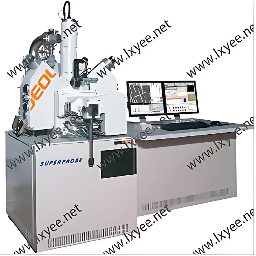

JEOL JXA-iHP100 Electron Probe Microanalyzer
| Brand | JEOL (Japan Electron Optics Laboratory) |
|---|---|
| Origin | Japan |
| Model | JXA-iHP100 |
| Acceleration Voltage | 0–30 kV (0.1 kV step) |
| Beam Current Range | 10⁻¹² – 10⁻⁵ A |
| Beam Current Stability | ±5% / h, ±0.3% / 12 h (W) |
| Secondary Electron Resolution | 6 nm (W), 5 nm (LaB₆) at WD = 11 mm, 30 kV |
| Scan Magnification | ×40 – ×300,000 (WD = 11 mm) |
| Max. Image Resolution | 5,120 × 3,840 pixels |
| Display | Dual LCDs (1,280 × 1,024 each) for EPMA and SEM/EDS operation |
| Optical Microscope Resolution | ~1 µm |
| Depth of Field | ~1 µm |
| Vacuum System | Mechanical pump + turbomolecular pump + ion pump |
| Chamber Vacuum | <8.0 × 10⁻⁴ Pa |
| Gun Vacuum | <9.0 × 10⁻⁵ Pa |
| Elemental Detection Range | WDS: Be (optional) to U |
| EDS | B to U |
| WDS Wavelength Range | 0.087–9.3 nm |
| EDS Energy Range | 0–20 keV |
| WDS Spectrometer Channels | 1–5 (configurable) |
| EDS Detector | One SDD (Silicon Drift Detector), fanless option available |
| Max. Sample Size | 100 mm × 100 mm × 50 mm (H) |
Overview
The JEOL JXA-iHP100 Electron Probe Microanalyzer (EPMA) is a high-precision, dual-mode microanalytical instrument engineered for quantitative elemental analysis at sub-micrometer spatial resolution. Based on the fundamental principles of electron–solid interactions, the JXA-iHP100 generates characteristic X-rays through electron beam excitation of solid specimens, enabling both wavelength-dispersive spectroscopy (WDS) and energy-dispersive spectroscopy (EDS) within a single platform. Its design integrates a thermionic LaB₆ or tungsten (W) electron source with a fully computer-controlled electron optical column, delivering stable probe currents from 10⁻¹² A to 10⁻⁵ A across an acceleration voltage range of 0–30 kV. This operational flexibility supports rigorous compositional mapping, phase identification, and trace-element quantification in geological, metallurgical, ceramic, semiconductor, and advanced materials research laboratories—particularly where regulatory compliance (e.g., ISO/IEC 17025, ASTM E1508, ASTM E2523) and long-term measurement reproducibility are required.
Key Features
- Hybrid WDS/EDS architecture: Supports simultaneous or sequential acquisition using up to five WDS spectrometers and one high-resolution silicon drift detector (SDD), with optional fanless cooling for ultra-low noise performance.
- User-defined analytical workflows: “User Recipes” allow full parameter preservation—including beam conditions, stage coordinates, spectrometer settings, and acquisition protocols—for rapid recall and cross-laboratory method transfer.
- Accelerated startup and point-and-analyze operation: Preconfigured EDS qualitative screening, quantitative ZAF/φ(ρz) correction routines, and WDS peak scanning can be initiated with a single mouse click on any region of interest.
- Dual-display control interface: Dedicated 1,280 × 1,024 LCD monitors for real-time EPMA data visualization and independent SEM/EDS navigation—reducing operator cognitive load during multi-technique sessions.
- High-stability electron optics: Beam current stability of ±0.3% over 12 hours (at constant working distance and temperature) ensures consistent count rates and minimizes recalibration frequency in GLP/GMP environments.
- Ultra-high vacuum architecture: Triple-pump system (rotary, turbomolecular, and ion getter) maintains chamber pressure below 8.0 × 10⁻⁴ Pa and electron gun pressure below 9.0 × 10⁻⁵ Pa—critical for minimizing hydrocarbon contamination and optimizing X-ray peak-to-background ratios.
Sample Compatibility & Compliance
The JXA-iHP100 accommodates bulk specimens up to 100 mm × 100 mm × 50 mm (H), compatible with polished sections, thin foils, and coated conductive samples. Its WDS capability covers elements from beryllium (Be) to uranium (U), while EDS extends detection down to boron (B) under optimized conditions. All analytical modes comply with internationally recognized standards for microanalysis: ASTM E1359 (quantitative EPMA), ISO 22309 (electron probe microanalysis — general principles), and USP <1058> (analytical instrument qualification). Data acquisition logs include full audit trails (timestamped parameters, operator ID, calibration history), supporting FDA 21 CFR Part 11 compliance when integrated with validated LIMS or ELN systems.
Software & Data Management
JEOL’s proprietary EPMA software suite provides a unified environment for instrument control, spectral processing, matrix correction (ZAF and φ(ρz)), and spatial distribution mapping. Raw WDS scans and EDS spectra are stored in vendor-neutral formats (e.g., .raw, .eds, .tdf), ensuring interoperability with third-party quantification tools such as DTSA-II or Probe for EPMA. Digital pulse processing enables real-time dead-time correction and pile-up rejection. Full-spectrum imaging (WD/ED, stage scan, beam raster) allows correlation of topographic, compositional, and crystallographic information without repositioning. All data files embed metadata compliant with the IUPAC Analytical Chemistry Data Exchange Standard (ACDES).
Applications
- Geosciences: Quantitative mineral chemistry, zoning profiles in igneous and metamorphic minerals, melt inclusion analysis.
- Metallurgy & Materials Science: Phase constitution mapping in superalloys, intermetallic compound stoichiometry, segregation analysis at grain boundaries.
- Semiconductor & Thin-Film Characterization: Layer thickness verification via X-ray absorption edge modeling, dopant distribution profiling in SiC and GaN devices.
- Forensics & Archaeometry: Provenance studies of glass, ceramics, and pigments through trace-element fingerprinting.
- Quality Control in Additive Manufacturing: In-situ powder composition verification and post-build defect chemistry assessment.
FAQ
What is the minimum detectable concentration for trace elements using WDS on the JXA-iHP100?
Detection limits depend on element mass, matrix absorption, and counting time—but typically range from 10–100 ppm for most mid-Z elements under optimized conditions (e.g., 100 s live time, 10 nA beam, pure standard).
Can the JXA-iHP100 perform automated particle analysis?
Yes—via optional Particle Analysis Module (PAM), which integrates stage automation, backscattered electron (BSE) threshold segmentation, and rule-based classification of particle morphology and chemistry.
Is the system compatible with external EBSD or cathodoluminescence detectors?
The JXA-iHP100 features standardized flanges and signal synchronization ports (TTL triggers, analog outputs) for integration with commercial EBSD and CL systems—subject to mechanical clearance and vacuum compatibility verification.
Does JEOL provide application support for method development?
JEOL offers remote and on-site application assistance, including SOP development, interlaboratory validation, and training on ZAF/φ(ρz) corrections, standard selection, and uncertainty estimation per ISO/IEC Guide 98-3 (GUM).


