JFP MPPS Integrated Dicing, Breaking, Die Attach, and Bonding System
| Brand | JFP |
|---|---|
| Origin | France |
| Model | MPPS |
| Maximum Wire Saw Speed | 400 mm/s |
| Sample Stage | Vacuum-Chuck with Rotatable Platform (Max Ø200 mm) |
| Angular Adjustment Resolution | 0.006° (Range ±4°) |
| Scribing Stroke Length | 250 mm |
| Scribing Width | 240 mm |
| Positioning Accuracy | 0.01 mm |
| Max Sample Thickness | 10 mm |
| Adjustable Scribing Force | 5–581 g |
Overview
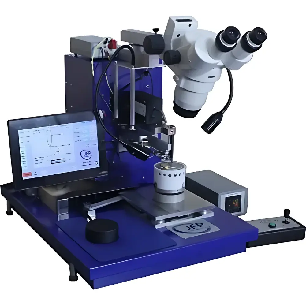
The JFP MPPS Integrated Dicing, Breaking, Die Attach, and Bonding System is a precision-engineered benchtop platform designed for semiconductor die-level processing in R&D laboratories and low-volume pilot production environments. Unlike conventional single-function tools, the MPPS consolidates four critical front-end packaging operations—mechanical scribing (diamond scriber-based), controlled die separation (breaking), adhesive dispensing and die placement (die attach), and thermocompression or epoxy-based bonding—into a single, space-efficient workstation. Its core scribing module operates on the principle of controlled mechanical scoring using diamond-tipped stylus tools under vacuum-stabilized substrate fixation. This method delivers repeatable groove geometry without thermal damage or subsurface microcracking—critical for brittle substrates such as silicon, SiC, GaN, fused silica, alumina, and LTCC ceramics. The system is not a laser dicer nor a plasma-based trenching tool; it relies on deterministic mechanical interaction, enabling high-fidelity process transfer from lab to qualification-grade prototyping.
Key Features
- Vacuum-chuck rotary stage (max Ø200 mm) with integrated angular indexing—enabling precise orientation alignment for anisotropic scribing patterns and multi-die array processing.
- High-resolution micrometer-driven angular adjustment (0.006° resolution, ±4° range) and vertical force control (5–581 g) for consistent groove depth and edge quality across diverse material hardnesses.
- X-Y translation stage equipped with machined V-grooves at 90° intervals, facilitating rapid mechanical registration of wafers, tiles, or pre-scribed substrates without optical recalibration.
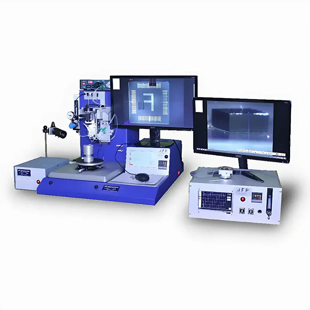
- Monocular crosshair microscope (standard magnification 10×–40×) with coaxial illumination, optimized for real-time visual confirmation of scribe line placement, crack propagation initiation, and bond alignment.
- Dedicated modular tooling stations: interchangeable diamond scriber holders, pneumatic breaking anvils with calibrated load feedback, non-contact adhesive dispensing nozzles (optional), and heated bonding platens (up to 300°C, ±0.5°C stability).
- Rigid granite base and linear-bearing motion architecture ensure long-term mechanical stability and sub-10 µm repeatability over extended operational cycles.
Sample Compatibility & Compliance
The MPPS accommodates rigid, flat substrates up to 10 mm thick and 200 mm in diameter—including silicon wafers (2″, 4″, 6″), ceramic substrates (Al₂O₃, AlN), glass wafers (borosilicate, quartz), and compound semiconductor blanks (GaN-on-Si, SiC). It complies with ISO 14644-1 Class 5 cleanroom compatibility when operated inside laminar flow hoods. All motion control firmware supports audit-ready logging per GLP/GMP guidelines, and optional configuration includes 21 CFR Part 11–compliant electronic signatures and data integrity modules. While not certified for high-volume manufacturing (HVM) inline integration, its process parameters are traceable to ASTM F39-22 (Standard Test Method for Scribe-and-Break Strength of Brittle Materials) and JEDEC JESD22-A113 (Die Shear Strength Testing).
Software & Data Management
The MPPS operates via embedded real-time motion controller with USB/RS-232 interface and optional Ethernet connectivity. A Windows-based host application provides intuitive workflow sequencing: scribe path definition (manual point-to-point or imported DXF), force/angle parameter presets per material type, break-cycle timing profiles, and bonding temperature ramp/soak schedules. All executed steps generate timestamped log files containing stage coordinates, applied force values, microscope focus position, and operator ID. Raw logs export to CSV or SQLite for integration into LIMS or MES platforms. No cloud dependency—data remains on-premise unless explicitly configured for secure FTP transfer.
Applications
- Research-scale fabrication of MEMS, power devices, and optoelectronic dies where laser dicing induces thermal stress or plasma etching causes sidewall charging.
- Prototyping of heterogeneous integration stacks (e.g., Si die bonded to glass interposers) requiring minimal kerf loss and no chipping at interface boundaries.
- Qualification testing of new die attach adhesives or transient liquid phase (TLP) bonding alloys under controlled thermal-mechanical boundary conditions.
- Failure analysis sample preparation—precise isolation of individual die without delamination or metallization pull-out.
- Academic teaching labs focused on semiconductor packaging fundamentals, offering hands-on exposure to full die singulation and interconnect workflows.
FAQ
Is the MPPS suitable for production-line integration?
No—it is engineered for R&D, qualification, and low-volume (<500 units/month) applications. Its manual alignment and sequential operation model prioritize flexibility and process transparency over throughput.
Can it process 8-inch wafers?
No. Maximum supported substrate diameter is 200 mm (8″). Larger formats require custom stage retrofitting, which voids factory calibration and compliance documentation.
Does it support automated vision-based alignment?
Not natively. The standard configuration relies on manual microscope alignment. Optional third-party machine vision add-ons (e.g., IDS Imaging USB3 cameras with OpenCV-based fiducial detection) can be integrated via GPIO triggers.
What diamond stylus specifications are recommended for SiC substrates?
A 30° included-angle mono-crystalline diamond tip with 50 µm radius and TiN coating is advised for optimal wear resistance and groove consistency on SiC (HV ~2500). Stylus replacement intervals are logged automatically based on cumulative scribe distance.
Is technical support available outside the EU?
Yes—JFP provides remote diagnostics and application engineering support globally via secure TeamViewer sessions and documented SOP libraries. On-site service requires advance scheduling and customs-compliant shipping of diagnostic toolkits.


