Klocke Nanotechnik KLOCKE 3D Nanofinger Nanoscale Coordinate Measuring Profilometer
| Brand | Klocke Nanotechnik |
|---|---|
| Origin | Germany |
| Product Type | Contact-Mode 3D Profilometer / Surface Topography & Roughness Measuring System |
| Measurement Range (X/Y/Z) | 10–50 mm / 10–50 mm / 10–20 mm |
| Extended XY Travel | 100 × 100 mm² or 350 × 350 mm² |
| Motion Resolution | 1 nm |
| Tip Resolution | 0.5 nm |
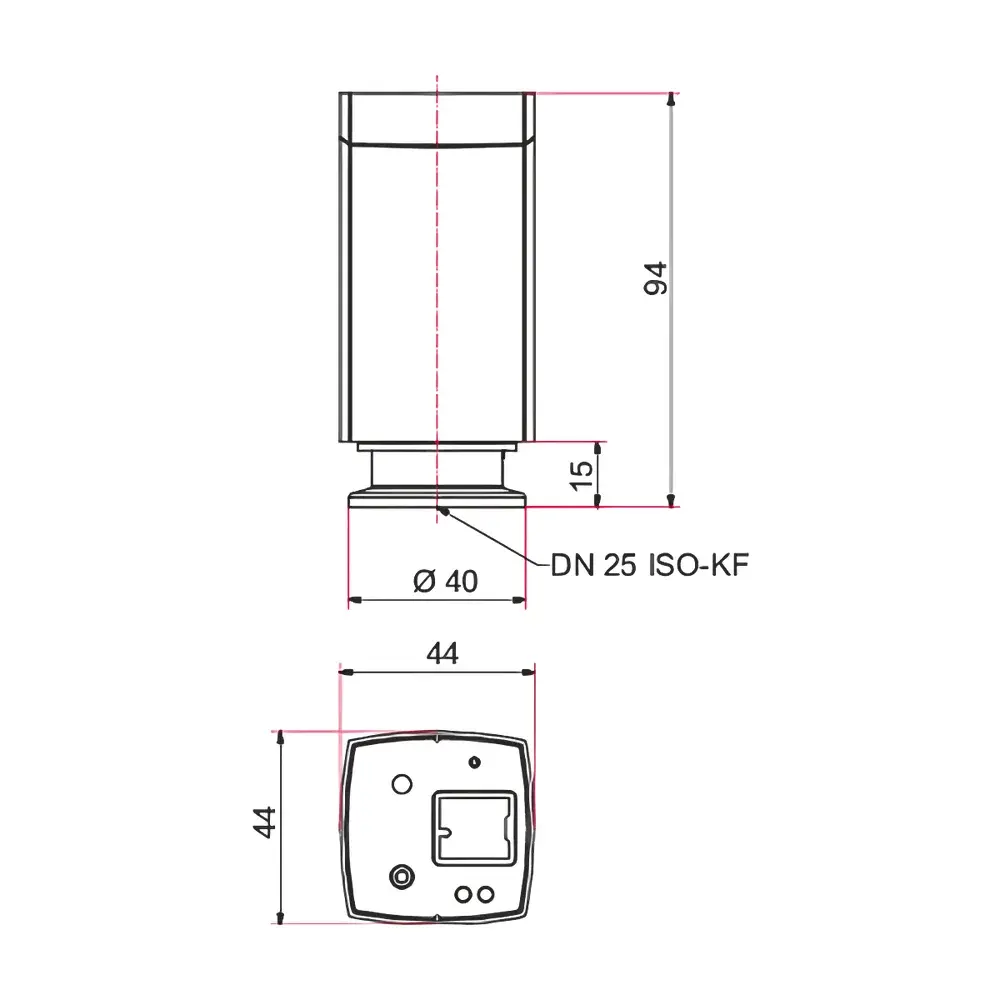
| Probe Types | Metallic wire tip (radius < 100 nm), hook-type wire tip (radius < 100 nm), spherical tip (Ø 0.12–0.3 mm), diamond tip (for indentation) |
| Sensor Configuration | Dual-axis (horizontal & vertical) capacitive displacement sensors |
| Software Features | Automated tip calibration & approach, 2D/3D visualization, quantitative surface analysis, optional sequence generator for automated measurement routines |
Overview
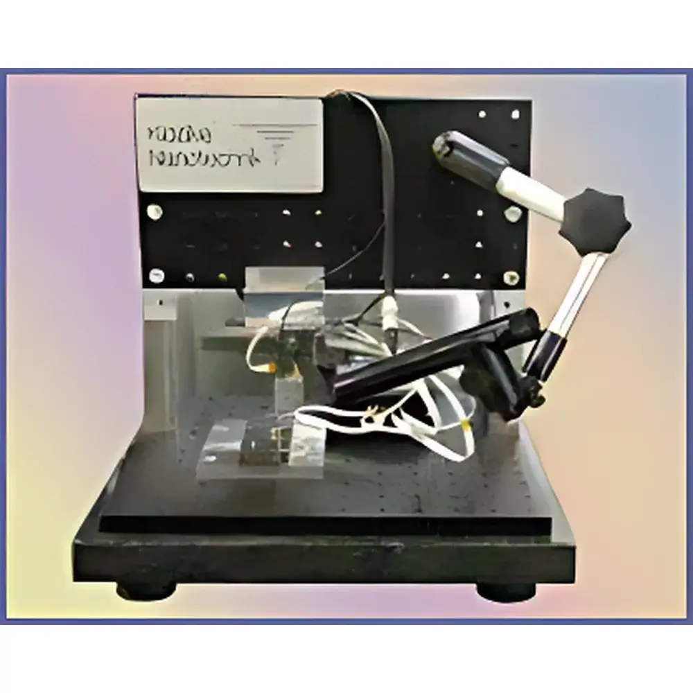
The Klocke Nanotechnik KLOCKE 3D Nanofinger is a high-precision, multi-degree-of-freedom coordinate measuring profilometer engineered for nanoscale metrology across three orthogonal axes. Based on contact-mode scanning with calibrated mechanical probing and closed-loop capacitive displacement sensing, the system delivers traceable, sub-nanometer resolution in all spatial dimensions—without reliance on optical diffraction limits or thermal stability constraints typical of interferometric or AFM-based platforms. Its rigid granite base, thermally stable kinematic design, and integrated 5-axis motion control (X, Y, Z, tilt, rotation) enable deterministic path planning over complex topographies—from microstructured semiconductor surfaces to MEMS cavity walls and precision optical aspheres. Unlike conventional CMMs limited to discrete point sampling or stylus profilometers restricted to 2D line scans, the 3D Nanofinger performs continuous, programmable areal profiling with simultaneous coordinate registration, supporting both dimensional verification and surface texture characterization under a single measurement framework.
Key Features
- Nanoscale resolution maintained uniformly in X, Y, and Z: motion resolution of 1 nm; tip displacement resolution of 0.5 nm
- Modular mechanical architecture with configurable travel ranges: standard stages (10–50 mm per axis); extended granite platforms (up to 350 × 350 mm² XY coverage)
- Multi-probe compatibility: interchangeable metallic wire tips (radius < 100 nm), hook-shaped probes for undercut and internal feature access, spherical tips (0.12–0.3 mm Ø) for curvature-sensitive profiling, and diamond-tipped variants for localized mechanical testing
- Dual-axis capacitive sensor feedback on both lateral and vertical axes ensures real-time force regulation and maintains consistent probe-sample standoff distance—typically adjustable from 2 nm to several micrometers
- Programmable measurement strategy support: hierarchical scanning (coarse survey followed by targeted high-resolution sub-area mapping), adaptive path generation along user-defined contours, and dynamic step-size modulation based on local surface gradient
- Open mechanical interface for integration: compatible with vacuum chambers, SEM sample stages, CNC machine tool beds, and multi-sensor metrology workbenches
Sample Compatibility & Compliance
The 3D Nanofinger accommodates solid-state specimens without material-specific constraints—suitable for conductive and non-conductive substrates including silicon wafers, fused silica optics, hardened steel tooling, polymer microfluidic chips, and ceramic MEMS packages. Its non-destructive, low-force contact mode (< 10 µN typical) prevents plastic deformation of soft materials while retaining fidelity on hard, brittle surfaces. The system complies with ISO 25178-2 (Geometrical product specifications — Surface texture: Areal — Part 2: Terms, definitions and surface texture parameters) and supports traceable calibration per ISO/IEC 17025-accredited procedures. When deployed in regulated environments (e.g., semiconductor fab QA labs or medical device manufacturing), measurement data logs—including tip calibration history, environmental drift compensation records, and operator audit trails—can be structured to satisfy FDA 21 CFR Part 11 requirements when paired with validated software modules.
Software & Data Management
Klocke’s proprietary Nanofinger Control Suite provides full instrument orchestration via deterministic real-time motion control firmware. Core capabilities include automated tip approach and contact detection, dynamic probe alignment compensation, and synchronized acquisition of position-encoded topographic data at up to 10 kHz sampling rates. The analysis engine computes ISO 4287/ISO 25178-compliant roughness parameters (Sa, Sq, Sz, Sdr), form deviation maps, curvature distribution histograms, and GD&T-referenced geometric tolerances (e.g., flatness, cylindricity, profile of a line/surface). All datasets are stored in vendor-neutral HDF5 format with embedded metadata (timestamp, environmental conditions, probe ID, calibration certificate hash). Optional Sequence Generator module enables unattended batch measurement workflows compliant with GLP/GMP documentation standards—including electronic signatures, version-controlled script libraries, and change-log auditing.
Applications
- Process validation and in-line inspection of ultra-precision machined components (e.g., diamond-turned infrared optics, micro-grooved bearing surfaces)
- MEMS device characterization: sidewall angle quantification, release etch depth uniformity, comb-drive gap metrology
- Semiconductor packaging: solder bump height/volume, underfill fillet geometry, TSV coplanarity assessment
- Biomedical microstructures: stent strut thickness variation, micro-porous scaffold interconnectivity, dental implant surface texturing
- Calibration artifact verification: step-height standards, roughness reference samples, sphere diameter artifacts per PTB/NIST traceability chains
- Research-grade surface science: wear track morphology evolution, thin-film delamination mapping, nanoimprint lithography fidelity analysis
FAQ
Is the 3D Nanofinger capable of measuring enclosed or recessed features?
Yes—the system supports specialized hook-type and miniature wire probes designed to access undercuts, blind holes, and internal microchannels with tip radii below 100 nm. Path planning accounts for probe geometry and collision avoidance in real time.
Can measurement data be exported for third-party analysis?
All raw and processed data are exportable in ASCII, CSV, and HDF5 formats. Metadata fields include coordinate frame definitions, probe convolution models, and environmental compensation coefficients—enabling interoperability with MATLAB, Python (NumPy/SciPy), and commercial metrology software such as MountainsMap® or PolyWorks®.
What environmental conditions are required for optimal performance?
The system operates reliably in standard laboratory environments (20 ± 1 °C, < 45% RH, vibration-isolated optical table recommended). For sub-nanometer repeatability, active air suspension and temperature stabilization are advised; optional thermal drift compensation algorithms reduce positional drift to < 0.3 nm/°C over 8-hour runs.
Does Klocke provide calibration services and traceable certificates?
Yes—factory calibration is performed using NIST-traceable step-height and roughness standards. On-site recalibration and ISO/IEC 17025-certified calibration reports are available through Klocke Nanotechnik’s global service network.