Klocke Nanotechnik Nano Positioning System
| Brand | Klocke Nanotechnik |
|---|---|
| Origin | Germany |
| Type | Precision Piezo-Based Nanopositioning Platform |
| Model | Klocke Nano Positioning |
| Compliance | Designed for UHV, Cryogenic, and High-Magnetic-Field Environments |
| Max Load Capacity | 2 kg |
| Travel Range | 5–70 mm |
| Velocity | < 2 mm/s |
| Open-Loop Motion Resolution | 2 nm |
| Sensor Resolution (Closed-Loop) | < 10 nm |
| Degrees of Freedom | XYZ linear, Θ/Φ rotation, XY/Z scanning, hybrid coarse/fine modes |
| Customization | Fully configurable mechanical design, material options (Invar, titanium, ceramics), vacuum-compatible variants, integrated metrology interfaces |
Overview
The Klocke Nanotechnik Nano Positioning System is a high-precision, piezoelectric-driven motion platform engineered for sub-nanometer spatial control in demanding scientific and industrial environments. Based on direct-drive capacitive-sensor feedback and low-drift ceramic actuator architecture, it operates on the principle of electrostrictive displacement amplification—enabling deterministic, hysteresis-free positioning without mechanical transmission elements. Unlike conventional motorized stages or voice-coil actuators, this system delivers true atomic-scale resolution with zero backlash, thermal drift compensation, and immunity to electromagnetic interference. It is specifically developed for integration into ultra-high-vacuum (UHV) chambers, cryostats operating below 4 K, and high-field magnet systems (up to 16 T), where conventional positioning solutions fail due to outgassing, thermal contraction mismatch, or Lorentz-force-induced instability.
Key Features
- True nanometer-scale open-loop resolution of 2 nm, with closed-loop sensor resolution better than 10 nm using integrated capacitive or interferometric position sensing
- Multi-axis configurability: modular XYZ linear stages, rotary (Θ/Φ) platforms, and hybrid coarse/fine architectures supporting simultaneous macro- and micro-positioning within a single unit
- Extreme-environment compatibility: all-metal vacuum-sealed construction; optional Invar or titanium frames; bakeable to 150 °C; certified for UHV (<1×10⁻¹⁰ mbar) and liquid nitrogen immersion
- No high-voltage drive required: operates from standard ±10 V analog input or digital EtherCAT interface, reducing EMI risk and simplifying integration with SEM, TEM, FIB, and AFM control ecosystems
- High static load capacity up to 2 kg—exceeding self-weight by 3–5×—with maintained positional stability over extended dwell times (>24 h)
- Zero mechanical hysteresis and negligible thermal drift (<0.1 nm/°C over operational range), validated per ISO 230-2 Annex B test protocols
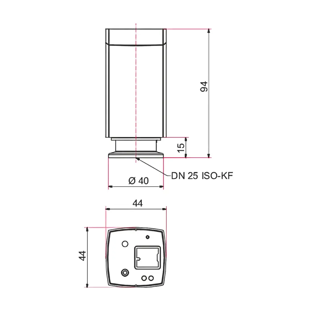
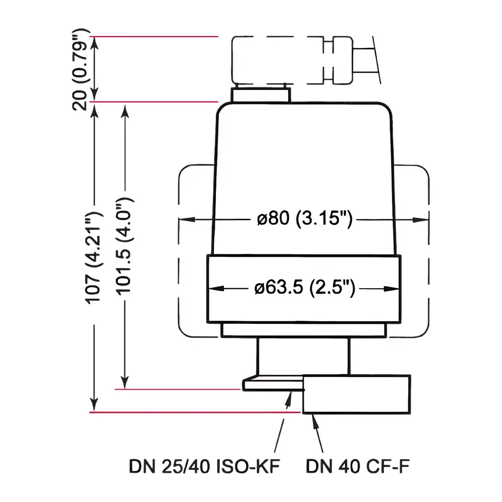
Sample Compatibility & Compliance
The Klocke Nano Positioning System is compatible with a broad spectrum of sample carriers, probe holders, and detector mounts used in electron microscopy, synchrotron beamlines, quantum device fabrication, and nanomechanical testing. Its mechanical interface conforms to standard M3/M4 tapped holes and kinematic mounting patterns (e.g., Ø6 mm dowel pin alignment). All variants comply with ISO 14001 environmental manufacturing standards and meet material outgassing requirements specified in ESA ECSS-Q-ST-70-02C for space-qualified instrumentation. Vacuum-rated models are tested per ASTM E595 for total mass loss (TML) and collected volatile condensable materials (CVCM), reporting TML < 0.5% and CVCM < 0.1%. For regulated laboratories, optional firmware supports audit-trail logging and user-access controls aligned with FDA 21 CFR Part 11 and EU Annex 11 principles.
Software & Data Management
The system integrates natively with Klocke’s NanoControl Suite—a cross-platform application supporting Windows, Linux, and real-time RTX environments. It provides deterministic motion sequencing (sub-millisecond jitter), synchronized trigger I/O for external detectors (e.g., photon counters, lock-in amplifiers), and programmable trajectory generation (sine, sawtooth, Lissajous, custom CSV-defined paths). Data export supports HDF5 and MAT formats for MATLAB/Python post-processing. Optional SDKs enable integration with LabVIEW, Python (PyVISA, NumPy), and EPICS-based control frameworks. Closed-loop operation includes real-time error correction with configurable PID tuning and dynamic bandwidth adjustment (1 Hz to 5 kHz), ensuring stability under variable inertial loading conditions.
Applications
- In situ TEM/SEM nanomanipulation: precise tip-sample approach, electrical contact formation, and mechanical property mapping at atomic scale
- Quantum transport experiments: positioning of gate electrodes, superconducting resonators, or spin qubit substrates inside dilution refrigerators
- Nanoimprint lithography alignment: sub-10 nm overlay accuracy across 70 mm travel range with thermal drift compensation
- Interferometric metrology: active vibration cancellation and path-length stabilization in gravitational wave detector prototypes
- Biophysical force spectroscopy: integration with optical tweezers or magnetic tweezers for dual-mode pN–nN force calibration
- Advanced semiconductor metrology: wafer-stage positioning for maskless e-beam lithography and defect review tools
FAQ
Is the Klocke Nano Positioning System compatible with ultra-high-vacuum systems?
Yes—standard configurations are UHV-rated (<1×10⁻¹⁰ mbar), with non-outgassing materials, metal seals, and no internal lubricants or adhesives.
Can it operate at cryogenic temperatures?
All base models function reliably down to 4 K; cryo-optimized variants with thermal contraction-matched actuators and sensors are available for sub-10 K applications.
Does it support closed-loop operation with third-party sensors?
Yes—the controller features analog input channels for external capacitive, LVDT, or laser interferometer signals, enabling full custom metrology integration.
What is the maximum payload for rotational modules?
Rotary stages support up to 1.2 kg at center-of-mass while maintaining <5 µrad angular drift over 12 hours at 23 °C.
Are OEM integration services available?
Klocke Nanotechnik offers full mechanical, electrical, and firmware co-design support—including custom flange interfaces, embedded FPGA logic, and qualification testing per customer-specific environmental profiles.