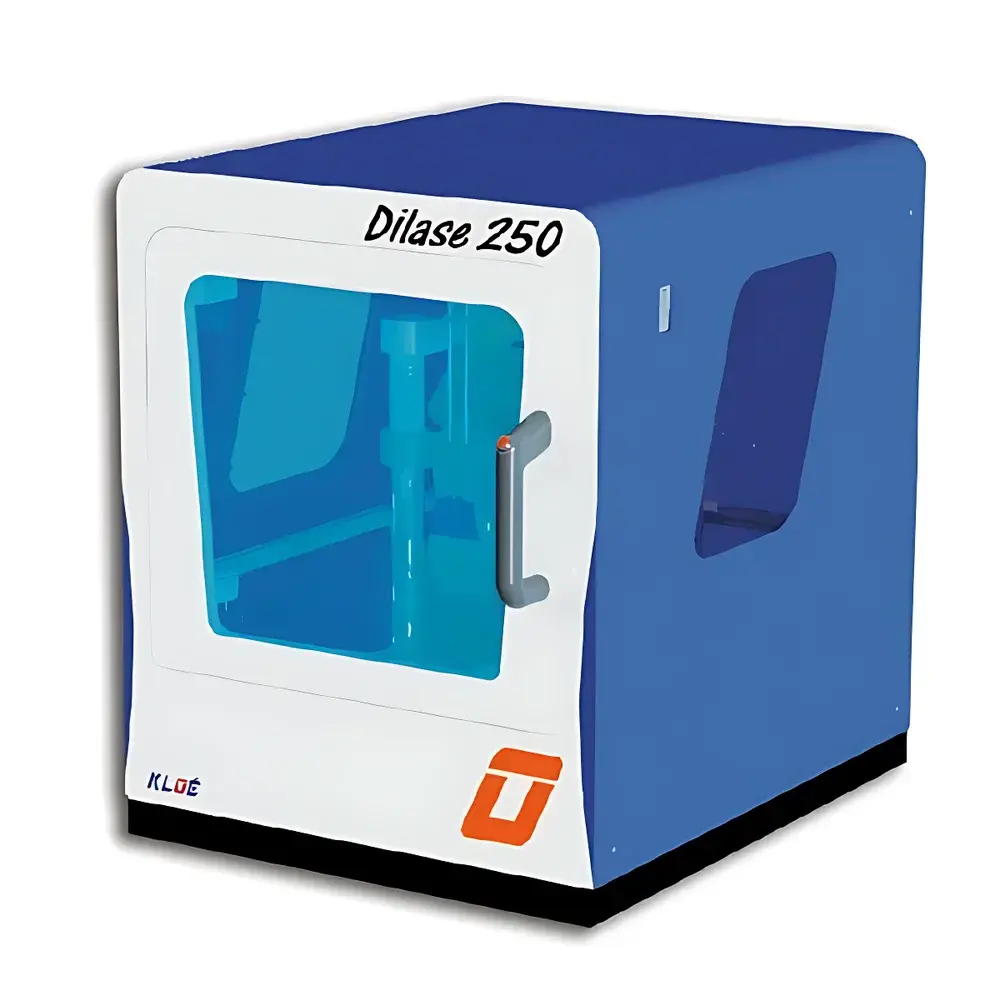
KLOE Dilase 250 Desktop Direct-Write Laser Lithography System
| Brand | KLOE |
|---|---|
| Origin | France |
| Model | Dilase 250 |
| Exposure Mode | Non-contact (Flying Spot) |
| Resolution | ≤100 nm (line width, under optimal resist & process conditions) |
| Wavelength | 375 nm or 405 nm (solid-state laser) |
| Beam Spot Size | Adjustable from 1 µm to 50 µm |
| Writing Area | 100 mm × 100 mm |
| Stage Positioning Accuracy | 100 nm (standard), 40 nm (optional) |
| Repeatability | ±100 nm |
| Overlay Accuracy (Multi-layer) | ≤1 µm |
| Orthogonality Error | <1 mrad |
| Maximum Sample Size | Up to 125 mm square (5-inch equivalent) |
| Substrate Thickness Range | 250 µm – 5 mm |
| Laser Lifetime | >10,000 h |
| File Format Support | GDSII, OASIS, DXF, LWO |
| Safety Compliance | EN 60825-1, IEC 61000-6-2/6-4, CE Marked |
Overview
The KLOE Dilase 250 is a high-precision, benchtop direct-write laser lithography system engineered for maskless patterning in R&D, prototyping, and low-volume microfabrication environments. Unlike contact or proximity aligners, the Dilase 250 employs a non-contact, flying-spot scanning architecture based on a collimated, diffraction-limited UV laser beam (375 nm or 405 nm). Its optical path — fully fixed and vibration-isolated — eliminates mechanical refocusing during exposure, enabling consistent depth-of-focus across large substrates. The system operates on the principle of serial raster or vector-based photochemical exposure: a digitally modulated laser spot is precisely positioned via galvanometric mirrors and/or high-resolution motorized stages, exposing photosensitive resists (e.g., SU-8, PMMA, AZ series) with sub-100 nm feature resolution under optimized process conditions. Designed for semiconductor, MEMS, photonics, and microfluidics laboratories, it bridges the gap between conventional photolithography and electron-beam systems — delivering nanoscale fidelity without vacuum infrastructure or conductive coating requirements.
Key Features
- Fixed-optics architecture with integrated solid-state UV laser (375 nm / 405 nm), eliminating thermal drift and alignment recalibration
- Hybrid motion control: high-speed galvo scanning combined with ultra-stable air-bearing or piezo-enhanced linear stages (100 nm standard, 40 nm optional resolution)
- True large-area writing: 100 mm × 100 mm continuous field without stitching artifacts, supported by granite base and active/passive anti-vibration design
- Three exposure modes — raster scan, vector scan, and hybrid scan+vector — enabling trade-off optimization between throughput (>100 mm/s linear speed) and critical dimension control
- Deep aspect ratio capability: validated for structures up to 20:1; customizable optics support up to 50:1 aspect ratio patterning via extended depth-of-focus beam shaping
- Full-spectrum safety integration: interlocked optical enclosure with IR/UV-blocking viewport, real-time door position monitoring, emergency stop circuitry, and Class 1 laser enclosure compliance per EN 60825-1
Sample Compatibility & Compliance
The Dilase 250 accommodates rigid substrates ranging from 3 mm × 3 mm chips to 125 mm square wafers (including 4″ and 5″ equivalents), with thicknesses from 250 µm to 5 mm. It supports standard lithographic materials including positive/negative tone resists (e.g., Shipley S18xx, MicroChem SU-8, Allresist AR-P/N), metal precursors, and hybrid organic-inorganic sol-gels. The system meets electromagnetic compatibility (IEC 61000-6-2/6-4) and laser safety standards (EN 60825-1), carries CE marking, and is compatible with cleanroom Class 100–1000 environments. While not certified for GMP production lines, its deterministic exposure algorithm, audit-ready log files, and deterministic file import (GDSII/OASIS/DXF) support GLP-aligned documentation workflows required for academic publication and pre-fab qualification.
Software & Data Management
DilaseSoft — the proprietary control and layout software — provides full workflow integration from design import to exposure validation. It natively reads GDSII, OASIS, DXF, and LWO formats, includes hierarchical flattening, dose calibration mapping, proximity effect correction (PEC) preview, and layer alignment simulation. Real-time exposure logging records timestamped parameters (laser power, stage coordinates, dwell time, shutter status), supporting traceability for ISO/IEC 17025-compliant labs. Export options include CSV metadata logs and PNG/SVG overlays for post-process metrology correlation. No cloud dependency: all processing occurs locally; data remains on-site unless explicitly exported. Software updates are delivered via secure offline installer packages, ensuring regulatory stability in controlled environments.
Applications
- Rapid prototyping of photomasks and reticles for maskless lithography test runs
- Micro-optics fabrication: diffractive optical elements (DOEs), microlens arrays, and waveguide couplers
- MEMS device patterning: accelerometers, pressure sensors, and RF resonators requiring high-aspect-ratio features
- Lab-on-chip and microfluidic channel definition in glass, silicon, and polymer substrates
- Quantum device research: gate electrode definition for 2DEG structures, superconducting qubit layouts
- Educational platforms for nanofabrication training — offering hands-on exposure control without cleanroom overhead
FAQ
Is the Dilase 250 compatible with standard semiconductor photoresists?
Yes — it is validated with industry-standard UV-sensitive resists including SU-8, PMMA, AZ 1518, and ma-N series. Dose calibration curves are provided for common formulations.
Does the system require periodic optical realignment?
No — the monolithic, fixed-path optical train eliminates routine alignment. Only annual laser power verification and stage calibration are recommended per maintenance schedule.
Can multi-layer alignment be performed on the same substrate?
Yes — using fiducial-based registration with sub-micron overlay accuracy (≤1 µm), supported by built-in camera-assisted alignment routines.
What is the typical minimum feature size achievable?
Under optimized resist processing (e.g., high-resolution e-beam resist + controlled development), isolated lines down to 100 nm are routinely achieved; dense patterns may vary depending on resist contrast and proximity effects.
Is remote operation or automation integration supported?
Yes — TCP/IP API access enables integration with factory automation systems (SECS/GEM) and custom Python/Matlab scripts for batch job sequencing and metrology feedback loops.


