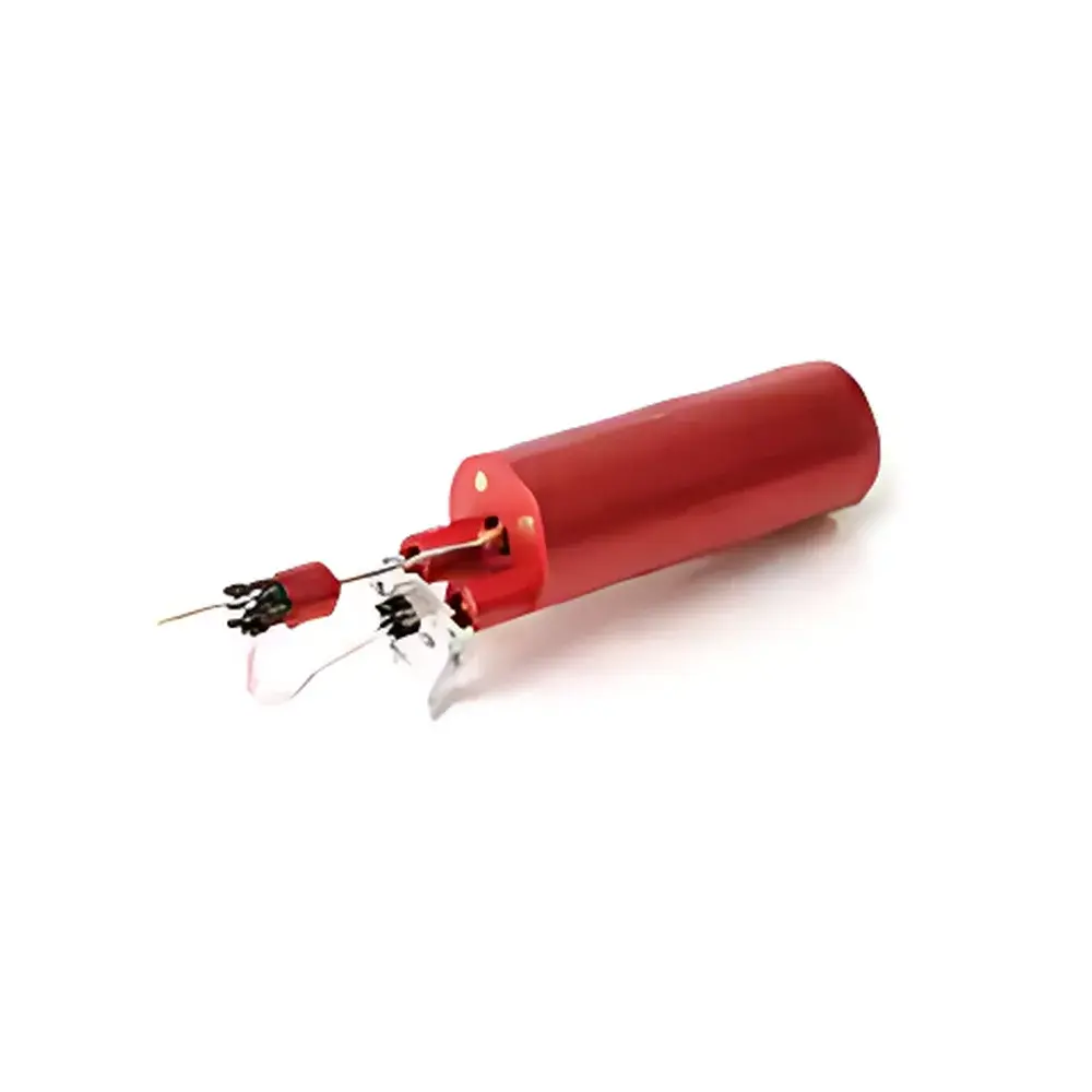
KP Kelvin Probe 020 Single-Point Scanning Kelvin Probe System
| Brand | KP (UK) |
|---|---|
| Origin | United Kingdom |
| Model | KP020 |
| Environment | Ambient & Controlled Atmosphere |
| Probe Options | 2 mm & 50 µm tip diameters |
| Work Function Resolution | 1–3 meV (2 mm tip), 5–10 meV (50 µm tip) |
| Tip-to-Sample Distance Control | Down to ≤400 nm |
| Height Regulation Mode (HR) | Active feedback-controlled vertical positioning |
| Detection Principle | Off-Null (ON) non-zero signal detection |
| Actuation | Voice-coil (VC) driver |
| Digital Control | Full digital parameter management (DC, SM, SA, WA, QT, DE, OC, FC, RS) |
| Software Export | Excel, Origin, third-party formats |
| Compliance | Designed for GLP-aligned surface potential mapping and work function metrology |
Overview
The KP Kelvin Probe 020 Single-Point Scanning Kelvin Probe System is a precision-engineered instrument for quantitative, non-contact, non-destructive measurement of surface potential and work function at solid interfaces. Based on the vibrating capacitor principle—where a conductive probe oscillates above a sample surface to modulate capacitance—the system detects contact potential difference (CPD) via electrostatic force feedback. This CPD directly correlates to the sample’s local work function (for conductors) or surface potential (for semiconductors and insulators), with sensitivity confined to the top 1–3 atomic or molecular layers. Unlike spectroscopic or sputtering-based techniques, Kelvin probe measurements preserve surface integrity and require no vacuum or conductive coating, making the KP020 especially suited for in situ and operando studies of functional surfaces under ambient, controlled-gas, or humidity-regulated conditions.
Key Features
- Off-Null (ON) Detection Architecture: Operates at high signal amplitude rather than null-balance (LIA-based) methods, delivering superior signal-to-noise ratio (SNR), immunity to low-frequency drift, and enhanced stability over extended acquisition periods.
- Active Height Regulation (HR) Mode: Integrated closed-loop z-position control maintains sub-400 nm tip-to-sample distance during scanning or point measurement—critical for eliminating topography-induced artifacts and ensuring reproducible CPD quantification across heterogeneous surfaces.
- Voice-Coil (VC) Actuation: Provides stable, linear, high-amplitude oscillation across broad frequency ranges (vs. piezoelectric drivers), enabling robust operation with variable tip geometries (2 mm and 50 µm), multi-probe configurations, and long-term mechanical reliability.
- Full Digital Parameter Management (DC): All operational parameters—including oscillation amplitude/frequency, gain, averaging window (SA), work function reporting mode (WA), user channel synchronization (UC), and TTL-triggered external circuit control (OC)—are programmable and logged via embedded firmware.
- Modular Hardware Integration: Includes color camera, adjustable focus lens, TFT display, Faraday cage (FC), gold-aluminum reference sample (RS), and quick-change tip mount (QT) for rapid spatial resolution adaptation (e.g., 2 mm for macro-scale screening; 50 µm for localized domain analysis).
- 24-Month Comprehensive Warranty: Covers electronics, mechanics, and calibration traceability—reflecting the system’s robust architecture and adherence to ISO/IEC 17025-aligned metrological practices for surface electronic property characterization.
Sample Compatibility & Compliance
The KP020 supports diverse sample classes without surface modification: metals, doped and intrinsic semiconductors, polymer films, oxide layers, biological membranes, corrosion-prone alloys, and photoactive thin-film stacks. It operates natively in ambient air and integrates seamlessly with optional environmental modules—including Relative Humidity Chamber (RH), Ambient Cell (AC) for gas-inlet control, and Surface Photovoltage (SPV) package for light-biased potential mapping. While not certified to ISO 17025 as a standalone calibration lab, the system meets essential requirements for GLP-compliant data generation: full audit trail (timestamped parameter logs), electronic signatures (via software export metadata), and traceable reference standards (RS). Its design facilitates alignment with ASTM E1938 (surface potential mapping), ISO 8256 (adhesion-related surface energetics), and USP <1058> guidelines for analytical instrument qualification in regulated R&D environments.
Software & Data Management
Data acquisition and visualization are managed through KP’s native Windows-based platform, supporting real-time CPD mapping, simultaneous topography correlation (via integrated height regulation), and dual-channel monitoring (e.g., CPD + external sensor input via UC). All raw and processed datasets export natively to CSV, Excel, Origin Lab, and HDF5 formats. Signal processing includes boxcar averaging (SA), work function differential/absolute reporting (WA), and stray-capacitance rejection via current-detection compensation (DC). The software enforces metadata tagging (operator ID, date/time, environmental conditions, probe ID) and permits batch processing of multi-region scans. For regulated environments, optional 21 CFR Part 11 compliance packages provide electronic signature workflows, role-based access control, and immutable audit logs—ensuring data integrity from acquisition through archival.
Applications
- Corrosion science: Localized Volta potential mapping of galvanic couples and passive film heterogeneity
- Battery research: In situ SEI evolution, anode/cathode interfacial band alignment, and charge transfer kinetics
- Organic electronics: Work function grading in OLED/OPV stack interfaces, dopant distribution analysis
- Catalysis: Surface dipole formation on supported nanoparticles and reaction-induced potential shifts
- Thin-film photovoltaics: Spatially resolved surface photovoltage (SPV) under calibrated illumination
- Nanomaterials: Fermi level pinning at quantum dot/matrix interfaces and graphene domain uniformity assessment
- Biointerfaces: Protein adsorption-induced surface potential changes and cell membrane potential screening
- Coating & adhesion: Surface energy gradients influencing primer bonding and delamination onset prediction
FAQ
What distinguishes Off-Null (ON) detection from conventional lock-in amplifier (LIA) approaches?
The ON method operates the probe at high oscillation amplitude and measures absolute CPD voltage directly—avoiding the noise-sensitive zero-crossing search inherent to LIA systems. This yields faster settling times (0.1–10 s per point), higher SNR, and reduced susceptibility to environmental drift.
Can the KP020 perform measurements inside gloveboxes or controlled-atmosphere chambers?
Yes—the system’s modular probe head and feedthrough-compatible cabling support integration into standard N₂/Ar gloveboxes and custom gas cells (optional AC module provides sealed inlet/outlet ports with mass flow control).
Is vacuum compatibility available for this model?
The KP020 is optimized for ambient and low-vacuum (<10⁻² mbar) operation. For UHV applications, KP offers dedicated UHV-KP systems with differential pumping stages and bakeable flanges—not included in the KP020 configuration.
How is spatial resolution determined, and what limits it?
Spatial resolution is governed by probe tip radius, tip-to-sample distance, and electrostatic field screening. With the 50 µm tip and HR-mode stabilization at ≤400 nm, lateral resolution approaches ~100 µm under optimal conditions—limited primarily by capacitive fringe-field spread rather than mechanical scanning fidelity.
Does the system support automated multi-point grid scanning?
Yes—programmable XYZ motion control (manual 25.4 mm stage included; motorized options available) enables user-defined raster patterns, region-of-interest mapping, and script-driven batch acquisition with synchronized data logging and metadata embedding.


