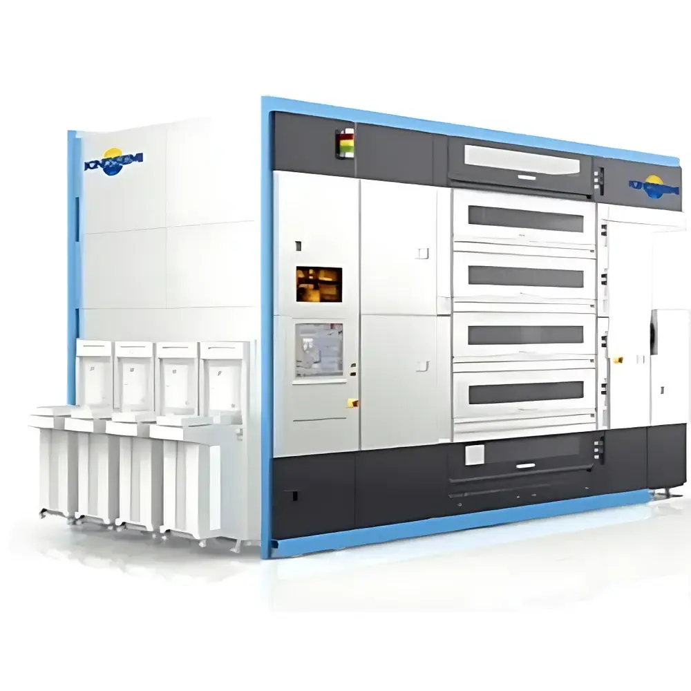
KS-FT200/300 Stackable Coater-Developer System for 8″ and 12″ Wafers
| Brand | Kingsemi |
|---|---|
| Origin | Liaoning, China |
| Model | KS-FT200/300 (8"/12" Front-End Process) |
| Application | ArF/KrF/I-Line photoresists, PI, BARC, SOC, SOD, SOG |
| Integration | Compatible with track-to-scanner inline lithography systems |
| Certification | Compliant with SEMI S2/S8 safety standards, ISO 14644-1 Class 5 cleanroom operation |
| Architecture | Modular stackable design |
| Thermal Control | Optional high-precision hot/cold plates (±0.1°C uniformity) |
| Inspection | Optional integrated Wafer Edge Exposure (WEE) and Automated Optical Inspection (AOI) modules |
| Maintenance | Front-accessible modular units with tool-less panel removal |
Overview
The KS-FT200/300 Stackable Coater-Developer System is a front-end semiconductor process tool engineered for high-throughput photolithography support in advanced IC fabrication facilities. Designed specifically for 200 mm and 300 mm wafer handling, it implements a dual-stage, vertically stacked architecture to maximize floor space efficiency while maintaining full process compatibility with sub-28 nm node technology nodes. The system performs sequential spin-coating, soft-bake (prebake), post-exposure bake (PEB), and aqueous or solvent-based development—each stage executed under tightly controlled environmental conditions including nitrogen-purged coating chambers, laminar airflow hoods, and temperature-regulated thermal plates. Its core functionality aligns with standard track-based lithography workflows, enabling seamless integration into automated factory environments via SECS/GEM communication protocols and standard mechanical interface (SMIF) or FOUP load ports.
Key Features
- Stackable dual-tier configuration reduces footprint by up to 40% compared to conventional horizontal layouts—critical for space-constrained cleanrooms.
- Multi-chamber shared dispense system with segmented retraction control minimizes photoresist waste and improves coating repeatability across wafer batches.
- Modular unit architecture supports field-upgradable configurations: thermal modules (hot/cold plates), edge-bead removal (EBR), wafer edge exposure (WEE), and AOI inspection can be added or repositioned without structural modification.
- Process chamber isolation meets ISO 14644-1 Class 5 requirements; all fluidic paths are constructed from PFA and quartz-compatible materials to prevent metallic contamination and ensure chemical resistance against aggressive developers (e.g., TMAH) and solvents.
- Real-time monitoring of spin speed (0–6,000 rpm), dispense volume (0.1–50 mL), bake temperature (ambient to 250°C), and chamber humidity (<2% RH) via embedded PLC with traceable logging.
Sample Compatibility & Compliance
The KS-FT200/300 accommodates standard 200 mm and 300 mm silicon, SOI, and compound semiconductor wafers—including those with high-aspect-ratio topography typical in MEMS and power device manufacturing. It supports both positive and negative tone resists across I-line (365 nm), KrF (248 nm), and ArF (193 nm) exposure wavelengths, as well as advanced organic planarization layers (SOC), spin-on dielectrics (SOD), and spin-on glass (SOG). All wet processing modules comply with SEMI F47 (electrical safety), SEMI S2 (health & safety), and SEMI S8 (ergonomics) standards. The system’s software architecture supports audit trails and electronic signatures per FDA 21 CFR Part 11 requirements when configured with validated GMP mode.
Software & Data Management
Equipped with Kingsemi’s proprietary TrackControl™ platform, the system provides recipe-driven operation with version-controlled process parameter sets, cross-chamber synchronization, and fault diagnostics with root-cause tagging. Data export adheres to SECS/GEM HSMS protocol for MES integration; log files include timestamped sensor readings (temperature, pressure, flow rate), actuator status, and error codes—all stored locally with optional cloud backup. Statistical process control (SPC) dashboards monitor coating thickness uniformity (via integrated metrology interface), develop time drift, and thermal plate stability over time—enabling predictive maintenance scheduling and OEE tracking.
Applications
This coater-developer system serves as a critical enabler in multiple advanced semiconductor domains: logic and foundry nodes down to 28 nm and beyond; CMOS RF transceivers requiring ultra-low defect density; high-voltage power ICs with thick resist stacks; MEMS inertial sensors and microfluidic devices demanding precise layer definition; NAND and NOR flash memory arrays; CMOS image sensors (CIS) with microlens and color filter patterning; display driver ICs for OLED and microLED backplanes; and heterogeneous integration platforms involving chiplet assembly and fan-out wafer-level packaging (FOWLP).
FAQ
Does the KS-FT200/300 support 300 mm wafer handling with FOUP automation?
Yes—it features dual-loadport capability compliant with SEMI E47.1 and supports both SMIF and FOUP carriers via robotic handler interface.
Can the system be retrofitted with AOI after initial installation?
Yes—its modular frame allows AOI module integration at any stage, with minimal downtime and no structural reinforcement required.
What level of temperature uniformity is achieved on the hot plates?
Standard configuration delivers ±0.3°C across 300 mm wafer surface; optional high-precision thermal modules achieve ±0.1°C with closed-loop PID control and real-time IR mapping.
Is the dispense system compatible with high-viscosity resists (e.g., >50 cP)?
Yes—the multi-segment retraction mechanism and pressure-regulated syringe pump enable stable dispensing of resists up to 120 cP without nozzle clogging or satellite droplet formation.
How does the system ensure process reproducibility across shifts?
Through automated calibration routines, hardware interlocks preventing parameter override, and encrypted recipe storage with role-based access control—fully aligned with ISO 9001 and IATF 16949 quality management frameworks.


