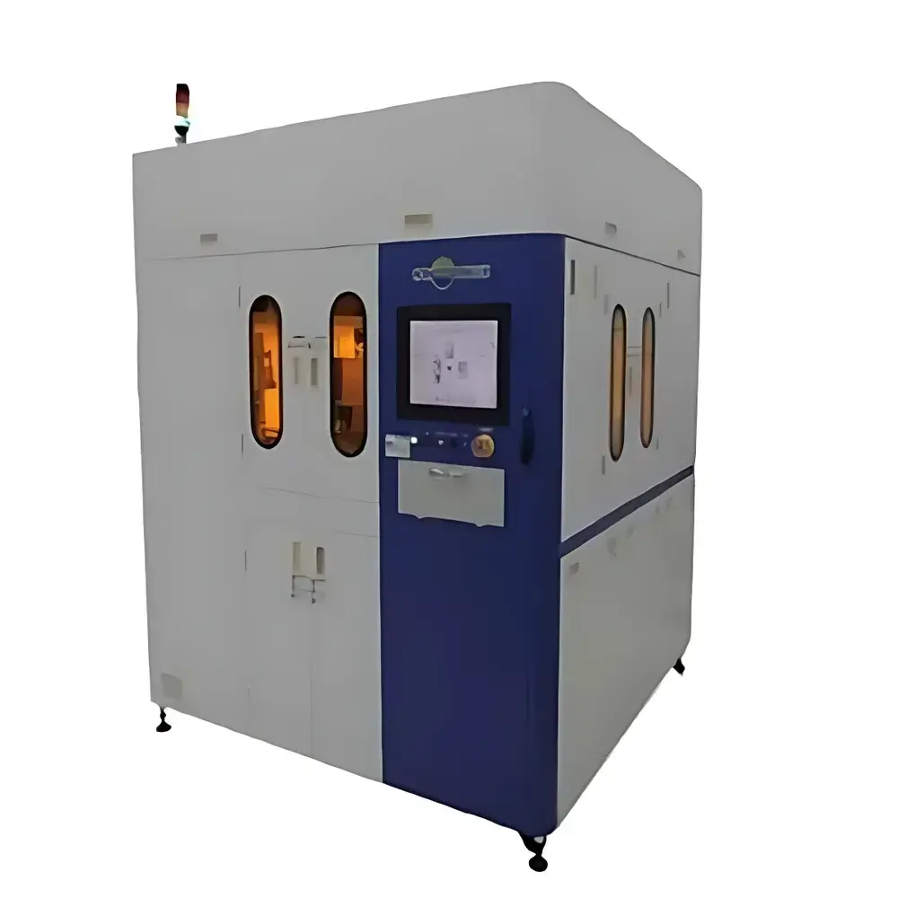
KS-S150 Star-Configuration Fully Automated Coater/Developer System
| Brand | Kingsemi |
|---|---|
| Model | KS-S150 |
| Configuration | Star-type fully automated coater/developer |
| Substrate Compatibility | Sapphire, GaAs, SiC wafers (4", 6") |
| Throughput | ≥190 wafers/hour (coating module) |
| Photoresist Consumption | 0.6 mL per 4" wafer |
| Certification | CSA Certified |
| Origin | Liaoning, China |
| Equipment Type | Semiconductor Coater/Developer for Patterning Processes |
| Application Scope | LED-PSS, compound semiconductor fabrication, sensor ICs, optical communication chips, power devices, patterned sapphire substrates |
Overview
The KS-S150 Star-Configuration Fully Automated Coater/Developer System is an integrated photolithography support platform engineered for high-precision, high-throughput resist processing in compound semiconductor and advanced optoelectronic manufacturing. Designed around a radial star-layout architecture, the system coordinates multiple process modules—including spin coating, soft bake, post-exposure bake, development, rinse, and hard bake—within a single, compact footprint. It operates on standard semiconductor cleanroom protocols and supports full automation via SECS/GEM interface compliance. The system implements laminar-flow optimized chuck design and closed-loop motorized dispensing control to ensure repeatable resist film formation across heterogeneous substrates including sapphire (Al₂O₃), gallium arsenide (GaAs), and silicon carbide (SiC). Its core function is to deliver uniform, defect-minimized photoresist films with precise thickness control and edge bead removal—critical prerequisites for sub-micron PSS (Patterned Sapphire Substrate) patterning and high-yield LED epitaxy.
Key Features
- Star-configuration modular layout enabling simultaneous parallel processing of up to six wafers across dedicated stations, minimizing idle time and maximizing tool utilization.
- High-accuracy dispense system with volumetric calibration traceability; achieves consistent 0.6 mL photoresist usage per 4-inch wafer—reducing material cost and waste generation.
- Thermally stabilized hotplates with ±0.3 °C uniformity over full chuck surface, supporting both soft bake (90–120 °C) and post-exposure bake (100–150 °C) profiles compliant with common i-line and UV resists.
- Integrated edge-bead removal (EBR) nozzle with programmable solvent flow rate and rotational speed synchronization, ensuring <5 µm edge exclusion zone.
- CSA-certified electrical safety architecture meeting Class 1, Division 2 hazardous location requirements for solvent-based processing environments.
- Modular maintenance design: all fluidic manifolds, chucks, and nozzles are accessible without disassembly of structural frames, reducing mean time to repair (MTTR).
Sample Compatibility & Compliance
The KS-S150 accommodates standard semiconductor wafer formats—4-inch and 6-inch diameters—with mechanical and vacuum-based clamping suitable for brittle substrates such as sapphire and SiC. Chuck temperature uniformity is validated per SEMI F47-0218, and resist thickness repeatability (3σ) is maintained at ≤1.2% across 49-point wafer maps. The system meets CSA C22.2 No. 61010-1 for laboratory equipment safety and incorporates leak-detection interlocks for developer and solvent lines. All wet process modules comply with SEMI S2/S8 environmental health and safety guidelines. While not FDA-registered, its architecture supports integration into ISO 9001- and IATF 16949-certified production lines where traceability and change control are enforced.
Software & Data Management
The KS-S150 runs on a real-time Linux-based controller with deterministic I/O response (<10 ms latency). Recipe management supports version-controlled parameter sets with audit trail logging per SEMI E10 and E142 standards. Each process step records timestamped metadata—including dispense volume, spin acceleration profile, thermal ramp rates, and chamber humidity—exportable via CSV or OPC UA to MES platforms. Optional 21 CFR Part 11-compliant software package provides electronic signatures, role-based access control, and immutable log archiving for GMP-aligned R&D and pilot-line deployment.
Applications
- LED manufacturing: PSS fabrication on sapphire wafers for improved light extraction efficiency in GaN-on-sapphire epitaxy.
- Compound semiconductor device processing: resist patterning for GaAs HBTs, InP-based photodetectors, and SiC power MOSFETs.
- Optical sensor fabrication: high-resolution lithography for MEMS-based spectral filters and VCSEL arrays.
- Power electronics: thick-film resist processing for trench gate etch masks in 650 V–1700 V SiC devices.
- Advanced packaging: redistribution layer (RDL) patterning on fan-out wafer-level substrates requiring tight CD uniformity and low defect density.
FAQ
What wafer sizes does the KS-S150 support?
The system is configured for 4-inch and 6-inch wafers, with chuck adaptability for non-standard geometries including square and rectangular substrates up to 150 mm diagonal.
Is the system compatible with aqueous and organic developers?
Yes—the fluid handling system supports both TMAH-based aqueous developers and organic solvents such as PGMEA and NMP, with chemically resistant PFA and EPDM wetted materials.
Can the KS-S150 be integrated into a factory automation environment?
It features SECS/GEM v5.0 communication protocol support, Ethernet/IP connectivity, and standard digital I/O mapping for seamless integration with host MES and AMHS systems.
Does the system include process qualification documentation?
Each unit ships with FAT (Factory Acceptance Test) report, wafer map uniformity data, thermal calibration certificates, and CSA test reports—all provided in English.
What is the typical preventative maintenance interval?
Recommended PM cycle is every 500 operating hours or quarterly—whichever occurs first—with documented procedures covering chuck cleaning, nozzle calibration, and bake plate emissivity verification.


