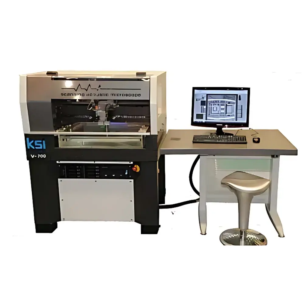
KSI V-700E Ultrasonic Scanning Acoustic Microscope (SAM)
| Brand | Analysis |
|---|---|
| Country of Origin | Germany |
| Model | KSI V-700E |
| Instrument Type | Digital |
| Inspection Method | Pulse-Echo |
| Waveform | Pulsed Ultrasound |
| Maximum Scan Area | 700 mm × 1000 mm |
| Gain Range | 0–120 dB |
| Dynamic Range | ≥40 dB |
| Resolution | ≥32 dB |
| Transducer Configuration | Single-Crystal |
Overview
The KSI V-700E Ultrasonic Scanning Acoustic Microscope (SAM) is a high-precision, non-destructive imaging system engineered for subsurface defect characterization in solid materials. Operating on the pulse-echo principle, it transmits high-frequency ultrasonic waves (up to 550 MHz bandwidth) into the sample and captures time-resolved acoustic reflections at material interfaces. Variations in acoustic impedance—caused by delaminations, voids, cracks, or interfacial debonding—generate amplitude and phase shifts in the returned signal, which are reconstructed into quantitative C-scan, B-scan, and depth-resolved volumetric images. Designed specifically for industrial R&D and failure analysis laboratories, the V-700E delivers sub-micron lateral resolution (down to 200 µm minimum scan field) and supports automated multi-layer scanning protocols. Its robust gantry architecture accommodates large-format samples up to 700 mm × 1000 mm, making it suitable for wafer-level inspection, power electronics qualification, and composite material integrity assessment without physical sectioning or sample preparation.
Key Features
- High-speed precision scanning with maximum velocity of 2000 mm/s and positional repeatability < ±1 µm
- Digital pulse-echo acquisition engine with 0–120 dB adjustable gain and ≥40 dB dynamic range for optimal signal-to-noise ratio across diverse material thicknesses and acoustic impedances
- FCT (Focused Crystal Technology) patented single-crystal transducer offering enhanced axial resolution and improved focusing stability over conventional piezoelectric elements
- Scalable scan area from 200 µm × 200 µm (micro-defect localization) to 700 mm × 1000 mm (full-panel or wafer-scale mapping)
- 625× effective magnification capability via digital zoom and interpolation algorithms compliant with ISO 17845 and ASTM E1783 standards for acoustic microscopy reporting
- Integrated environmental compensation for temperature-induced acoustic velocity drift during extended acquisition sequences
Sample Compatibility & Compliance
The V-700E is validated for use across semiconductor packaging (e.g., flip-chip solder bumps, underfill voids, die attach delamination), advanced power modules (IGBT substrates, ceramic-metal interfaces), MEMS devices, and structural composites (CFRP, metal matrix laminates). It complies with ISO/IEC 17025 requirements for calibration traceability and supports GLP/GMP documentation workflows. All image metadata—including transducer frequency, gate settings, gain profile, and scan parameters—is embedded in DICOM-SAM format for audit-ready archiving. The system meets IEC 61000-6-3 EMC emission limits and operates within Class I laser safety classification per IEC 60825-1 (no optical radiation hazard).
Software & Data Management
Acquisition and analysis are performed using KSI’s proprietary SAM Studio v5.x software suite, featuring real-time C-scan rendering, automated defect thresholding, and cross-sectional B-scan slicing with depth-gating. The platform supports 3D volume reconstruction with iso-surface rendering and quantitative metrics including void area %, delamination length, and crack density per unit area. Data export conforms to ASTM E2373 (Standard Practice for Reporting Acoustic Microscopy Data) and enables integration with LIMS and MES systems via OPC UA and HL7-compatible APIs. Audit trails record all user actions, parameter modifications, and image processing steps in accordance with FDA 21 CFR Part 11 requirements for electronic records and signatures.
Applications
- Semiconductor: Detection of interfacial voids in wafer bonding, solder joint fractures in 2.5D/3D IC stacks, and filler gel delamination in fan-out packages
- Power Electronics: Assessment of thermal interface material (TIM) bond quality in SiC MOSFET modules and copper sintering defects in DBC substrates
- Advanced Materials: Evaluation of porosity distribution in additively manufactured alloys, fiber-matrix debonding in carbon-fiber composites, and coating adhesion in PVD/CVD thin films
- Medical Devices: Non-invasive evaluation of hermetic seal integrity in implantable pacemaker housings and ultrasonic characterization of bioresorbable polymer scaffolds
- Automotive: Validation of adhesive bond strength in battery module cold plates and detection of microcracks in ceramic brake components
FAQ
What is the primary measurement principle used by the KSI V-700E?
It employs pulse-echo ultrasonic scanning, where broadband acoustic pulses are transmitted into the sample and reflected signals are analyzed for time-of-flight, amplitude, and phase changes at acoustic impedance discontinuities.
Can the system perform through-silicon via (TSV) inspection on 300 mm wafers?
Yes—the 700 mm × 1000 mm scan envelope accommodates full-wafer carriers, and the FCT transducer supports frequencies up to 550 MHz for sub-µm vertical resolution in silicon.
Is the software compliant with regulatory data integrity requirements?
Yes—SAM Studio implements role-based access control, electronic signatures, and immutable audit trails aligned with FDA 21 CFR Part 11 and EU Annex 11 guidelines.
Does the system support automated defect classification?
It provides configurable threshold-based segmentation and morphology filters; AI-assisted classification modules are available as optional add-ons validated per ISO/IEC 17065 for conformity assessment tools.
How is calibration maintained across long-term operation?
The system includes daily self-calibration routines using reference standards traceable to PTB (Physikalisch-Technische Bundesanstalt), with full calibration certificates issued per ISO/IEC 17025.


