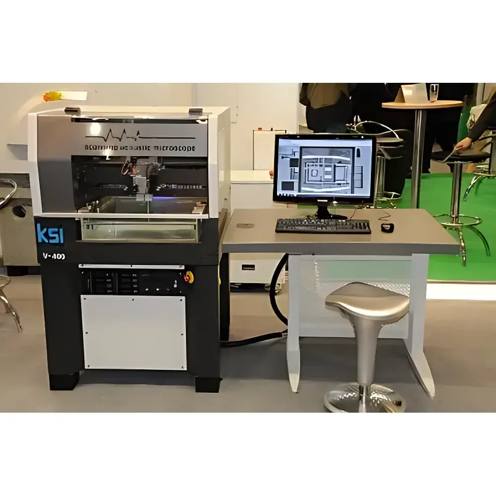
KSI V400E Ultrasonic Scanning Acoustic Microscope (SAM)
| Origin | Germany |
|---|---|
| Manufacturer Type | Authorized Distributor |
| Origin Category | Imported Instrument |
| Model | V-400E |
| Detection Method | Pulse-Echo Mode |
| Waveform Type | Pulsed Ultrasound |
| Maximum Scan Speed | 2000 mm/s |
| Minimum Scan Area | 200 µm × 200 µm |
| RF Bandwidth | 500 MHz |
| Probe Configuration | Single Transducer (Standard) |
| Frequency Range (Optional Probes) | 100–2000 MHz |
| Axial Resolution (Typical) | <100 nm (with Nano-series transducers) |
| Integrated Optical Microscopy | Yes (Inverted & Epi-Illumination Configurable) |
| Compliance | ASTM E1783, ISO 16932, IPC-J-STD-035, JEDEC JESD22-A108 |
Overview
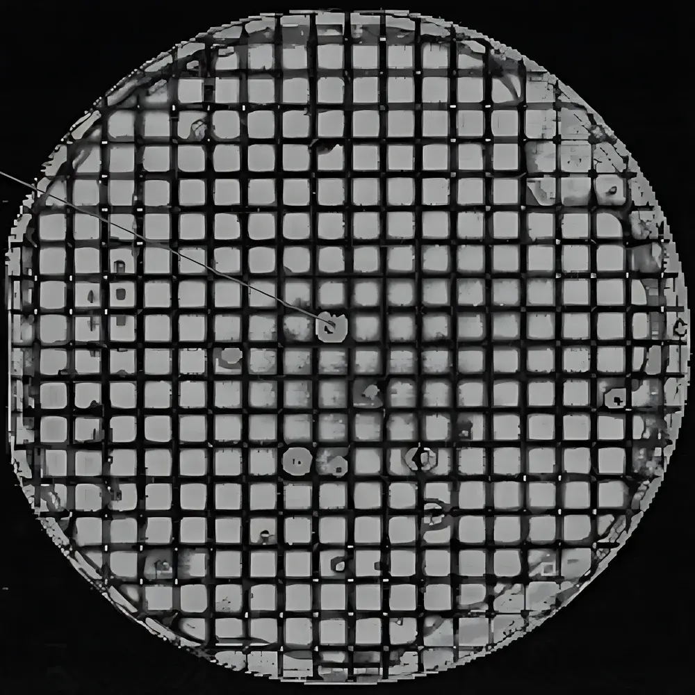
The KSI V400E Ultrasonic Scanning Acoustic Microscope (SAM) is a high-precision, non-destructive imaging platform engineered for sub-micron defect characterization in advanced materials and microelectronic packages. Operating on the pulse-echo principle, the system emits focused high-frequency ultrasound pulses (100 MHz to 2000 MHz) into the sample; acoustic impedance mismatches—caused by voids, delaminations, cracks, or interfacial discontinuities—generate time-resolved echo signals that are reconstructed into high-fidelity C-scan, B-scan, and through-focus volumetric images. Unlike destructive cross-sectioning or X-ray tomography, SAM provides quantitative, layer-specific structural information without sample preparation or ionizing radiation. Its integrated dual-modality architecture—combining synchronized acoustic and optical imaging—enables direct spatial correlation between mechanical integrity (acoustic contrast) and morphological features (optical contrast), making it indispensable for failure analysis, process validation, and reliability qualification in semiconductor packaging, advanced composites, and biomedical device manufacturing.
Key Features
- High-speed scanning capability up to 2000 mm/s with sub-micron positional repeatability (±0.1 µm), enabling rapid full-wafer or large-area package inspection
- Dual-path imaging engine: Simultaneous acquisition of RF ultrasonic data and high-resolution optical microscopy (inverted or epi-illumination, up to 1000× magnification)
- Proprietary FCT (False-Call Thresholding) probe technology minimizes false-positive indications from surface roughness or acoustic noise
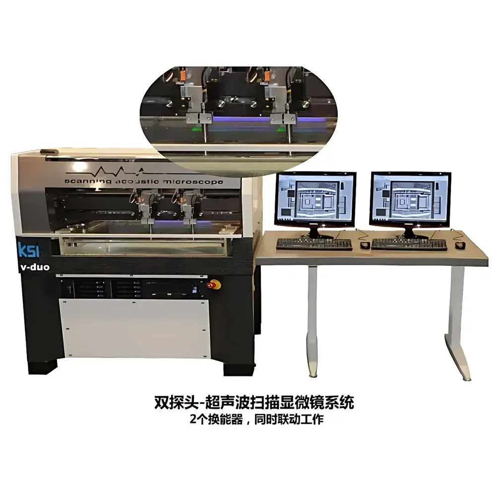
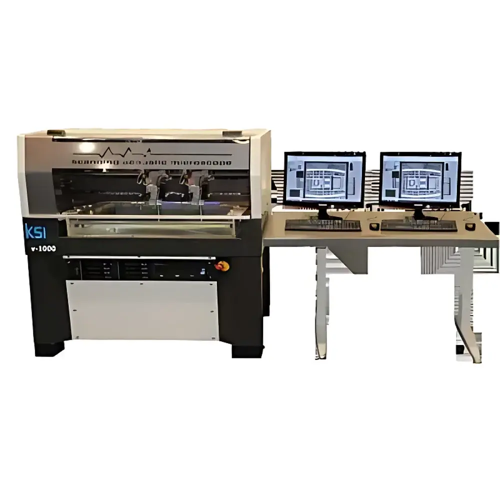
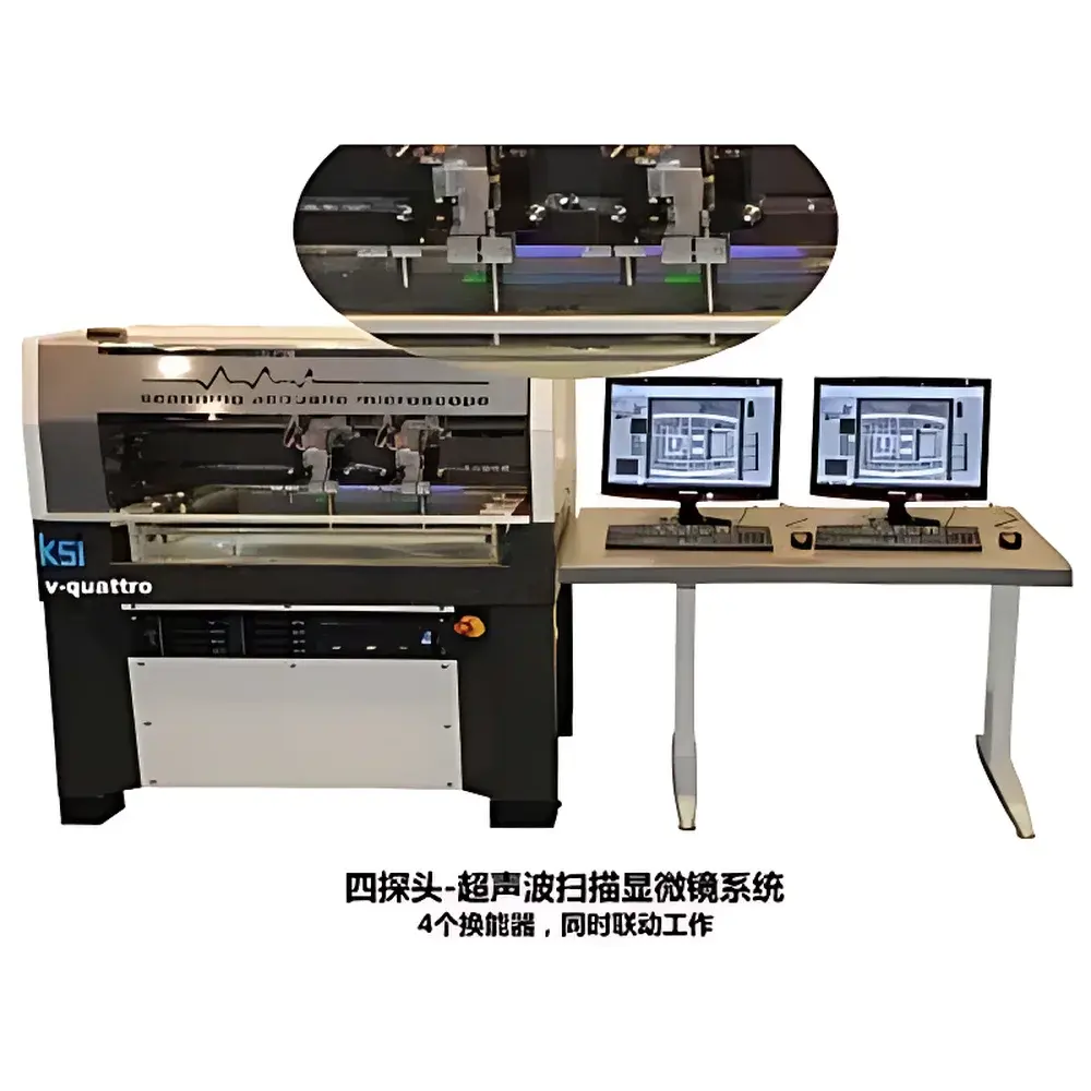
- Expandable transducer architecture supporting single (V-duo), quad (V-quattro), or octo (V-Octo) probe configurations for parallel multi-angle interrogation
- Ultra-wide RF bandwidth (500 MHz standard, 550 MHz optional) ensures optimal signal fidelity for both near-surface (1 mm) analysis
- Real-time acoustic impedance mapping and automated void area/percentage quantification compliant with IPC-J-STD-035 and JEDEC JESD22-A108 standards
Sample Compatibility & Compliance
The V400E accommodates rigid and semi-rigid specimens up to 300 mm × 300 mm × 50 mm (W × L × H), including silicon wafers (200 mm / 300 mm), molded IC packages (QFN, BGA, WLP), ceramic substrates, metal-matrix composites, and polymer-coated medical implants. All scanning protocols support water-coupled immersion mode with temperature-stabilized coupling baths (±0.1 °C). The system meets ISO/IEC 17025 traceability requirements for measurement uncertainty reporting and supports audit-ready documentation per FDA 21 CFR Part 11 (electronic signatures, audit trails) and GLP/GMP workflows. Calibration is performed using NIST-traceable reference standards (e.g., SiO₂ step-height wafers, stainless steel void arrays).
Software & Data Management
KSI AcousticStudio v8.2 software provides a unified interface for acquisition, reconstruction, annotation, and statistical reporting. It includes automated layer segmentation, depth-gated C-scan slicing, 3D volume rendering (DICOM export), and batch-mode analysis across multiple samples. Data integrity is ensured via encrypted project files with embedded metadata (operator ID, timestamp, instrument configuration, calibration status). Export formats include TIFF (8/16-bit), CSV (defect coordinates/metrics), PDF reports (with pass/fail thresholds), and HDF5 for integration with MATLAB or Python-based analytics pipelines. Software validation documentation (IQ/OQ/PQ) is available upon request for regulated environments.
Applications
- Semiconductor: Detection of die attach voids, mold compound delamination, TSV fill defects, and wafer-level bonding failures in 3D-IC and fan-out packaging
- Power Electronics: Assessment of solder joint integrity, copper pillar voiding, and thermal interface material (TIM) uniformity in IGBT modules and SiC devices
- Advanced Materials: Quantification of porosity distribution in additively manufactured alloys, fiber-matrix debonding in CFRP, and coating adhesion strength in thermal barrier systems
- Medical Devices: Non-invasive evaluation of hermetic seal quality in implantable electronics, hydrogel swelling behavior, and bone-implant interface integrity
- Research: Correlative studies linking acoustic attenuation spectra to local elastic modulus (via inverse modeling), nanoscale interfacial stiffness mapping, and time-resolved dynamic response under thermal or mechanical stress
FAQ
What is the minimum detectable void size with the V400E using a 1 GHz transducer?
Under optimal coupling and signal-to-noise conditions, lateral resolution approaches 1.5 µm; axial resolution is ~0.3 µm. Sub-100 nm thickness variations (e.g., thin film delamination) are resolvable via phase-sensitive detection modes.
Does the system support automated pass/fail classification based on IPC-A-610 or AEC-Q200 criteria?
Yes—customizable rule sets can be defined in AcousticStudio for real-time classification of void area, count, and location relative to critical features (e.g., bond pads, solder joints), with configurable tolerance bands and statistical process control (SPC) charting.
Can the V400E be integrated into an automated production line?
The system supports SECS/GEM protocol communication, PLC-triggered scanning sequences, and Ethernet/IP connectivity for MES integration. Optional robotic sample handling and barcode-driven recipe selection are available.
Is training and application support provided for failure analysis engineers?
KSI-certified application specialists deliver on-site installation qualification, method development workshops, and ongoing remote troubleshooting—including root cause interpretation of complex multi-layer echo patterns.
How is acoustic data calibrated for quantitative elastic property estimation?
While absolute modulus quantification requires complementary techniques (e.g., nanoindentation), the V400E’s calibrated RF amplitude and time-of-flight outputs enable relative stiffness mapping and comparative benchmarking across lots or process changes when combined with reference standards.


